The FV-1 based SDR revisited

I have really enjoyed my FV-1 based mini SDR radio but it has one problem…its too small! I made the thing so small; it’s hard to operate and assemble. So I decided to make it a little larger, allowing for all the controls to be larger and more spaced out. It has a larger display and the circuit board layout provides for the switches, encoder, volume control and display all to be soldered directly to the board. All of the circuit components are now on the top side of the board as well. Along with these physical changes, I made some minor circuit changes. These include: some component value changes, a different microcontroller, clocking the FV-1 at 48Khz with the third output of the SI5351 and adding a on/off power circuit which utilizes a momentary switch instead of a latching one. It now has a built in flat pack lithium ion battery that can be USB charged. I also refined the DSP demodulators and I am now utilizing a weaver demodulator for USB/LSB.

I started using a simple graphically based CAD tool(SPINCAD) to develop the demodulator DSP code for the FV-1, and I have been able to improve my demodulators algorithms. The CAD tool is free and is Java based. It runs natively in windows with Java installed. You can wire together functional building blocks and generate the required hex code for the FV-1 without writing any assembly code.

Examples of SPINCAD Graphical Programs

Link To Tech Data:

https://www.adrive.com/public/rPpBxR/MiniSDR%20Tech%20Data_11_2020.zip

High Efficiency 4V supply QRP Amplifier

This is an example of a high efficiency QRP transmitter designed to work at very low supply voltages (3v-5v). It can produce 2 watts a 4 volt supply @ 70% efficiency. It uses small, inexpensive switching mosfets. The primary requirement for these mosfets is low output capacitance, a VDS of >20V, a logic level VGS and a drain current rating of a couple amps. There are many devices that will work. Unlike a Class E amplifier, this design requires no special alignment, providing for multiband operation easily. Only the output filter consisting of a L Network and Pi network in series need to be changed for a given band. It is tolerant of all kind of load conditions including infinite Z and maintains efficiency when poorly matched. While this circuit utilizes a microcontroller, display and clk generator, the logic buffer can operate from any oscillator source so the amplifier can be adapted to simpler designs.

QRP Transmitter Schematic

Simple low current mini-whip antenna

I decided to try using a small  wide band E field type antenna with my newest receiver  design…the Mini SDR and the results have been gratifying. There many useful articles describing this type of antenna; so I won’t go into much detail about how it works. More or less it functions as  a capacitive E field probe and therefore is very sensitive to EMI. However, if placed outside away from house wiring and provided with a modest local ground reference..the antenna is a good performer. The classic circuit uses a JFET source follower and a BJT follower stage to provide impedance transformation of the Hi Z capacitive terminal to a 50 ohm Z drive for transmission line. This circuit works fine but has some drawback, namely requiring 65mA of current and having a somewhat large input capacitance, which reduces performance with frequency. I decided to use a wide bandwidth op amp to simplify the circuit, reduce current, and provide a little  voltage gain. The op amp I chose was one I have used before for RF amplification..the LT1818. When choosing an op amp for such an application..there are a few important criteria to focus on:

1. current noise: Unlike low impedance  topologies where voltage noise and resistor thermal noise will dominate, having a Hi Z input will make the current noise the dominant source of amplifier noise.

2. Bandwidth: you need a wide bandwidth on the order of hundreds of MHz or more to provide the required frequency response up to 30Mhz. This is especially true for voltage feedback op amps, where the phase shift compensation rapidly reduces performance over frequency.

3. Slew rate: You want the largest slew rate you can get to reduce distortion and IMD products.

4. Input bias current/ input Z/ input capacitance: You need low input capacitance so as to not to create a lossy divider with the antenna terminal. You want low input bias current and high input Z to not load down the terminal. If the input bias current is too high , then you need a low value  bias resistor which loads the terminal.

5. Low output impedance: To drive 50 ohm Z and minimize distortion.

The LT1818 has excellent specs with regard to all of these criteria. It can operate on 3v-12v and requires only 9mA of current to operate. The Amplifier will operate from VLF to beyond 30Mhz with no change in performance.

Schematic:

E Field Ant

The antenna is powered via a power splitter connected between the receiver and antenna. This is the purpose of L1 to isolate the DC power from the RF output from the antenna.

I 3D printed antenna capsule  from HIPS, which is a low RF loss material and used a 3″ square of PC board to create the capacitive antenna terminal.  The printing was done at 50% density so it’s a very light, low dielectric loss enclosure.

Installed Antenna(with LED illumination)

MVIMG_20200206_213153

Antenna Element

IMG_20200206_172500062


Complete 4″ x 1-1/2 inch antenna

IMG_20200206_172722888


Amplifier Circuit

IMG_20200206_172521323


Antenna Terminal

IMG_20200206_172412346


Efield Antenna Demo:


Si5351 based SDR Circuit Updates

I am going to be posting any tweaks, component changes and firmware/circuit mods here on this page.

02/02/2020: Changed the RF input buffer to a better performing amplifier with another option annotated as well. Also I changed some resistor values in this gain stage to  improve performance.

02/07/2020: Oops the integrating capacitors on the switching detector were shown as 1uF…it has been changed to the correct value of .1uF

02/07/2020: Updating the download link with the new schematic and an improved  AM demodulator for the FV-1.

Coming soon: New code for FV-1 based on 48Khz sampling…plus new schematic/layout utilizing the leftover SI5351 output as The FV-1 clk instead of a 40KHz xtal.

Newest Schematic here:

Updated Schematic


Compact Si5351 based SDR

Go here for the most up to date circuit /firmware mods: Design Updates

This is a revised version of my FV-1 based SDR. I replaced the CS2100 clk generator with the Si5351 clk generator. The Si5351 has some advantages over the CS2100, namely you can generate quadrature clks directly. This simplifies the hardware design and improves the quadrature accuracy. The sideband rejection in LSB/USB modes is impressive..somewhere around 60 db as best I can measure. The DSP processing is accomplished by the use of a FV-1 audio processor. The device makes the base band signal processing a snap. It requires some code to be loaded on a EEprom but the circuitry is simple and allows for up to 8 selectable programs. I created three: AM/USB/LSB . The FV-1 provides for three analog POT inputs to control any parameters you choose. Gain, variable filter bandwidth and depth, AGC are some examples of adjustable parameters if you desire. I kept it simple and created fixed band pass filters to taste. I did use one of the controls for AF gain. The design has no tuned circuits or band pass filters but they could easily be added.  It works just fine without them. Occasionally, I come across a ghost signal from harmonic mixing, when tuning, but not enough to matter. The design uses an OLED display and a rotary encoder for tuning. The frequency coverage is from 2.7 Mhz to 25Mhz. The bottom limit is created by the inability of the Si5351 to support quadrature below this frequency. Although I have improved my DSP programs for the FV-1 and have developed new display drivers and the new code for the Si5351, useful detail about using the Fv-1 can be found in my original design from a few years ago: https://circuitsalad.com/2015/06/19/comming-soon-stand-alone-software-defined-radio-baseband-demodulator-no-computer-required/

Schematic: Updated 05/17/2020

The design uses a LT1818 or THS4304 low noise op amp as an RF input with gain. It provides a constant and reliable resistive Rf termination for the sampling detector.  This allows for random antennas to be used without adversely affecting the input termination to the detector. All the code to operate the main processor(display/clk generator/tuning, band select and receive mode) was written in MikroC which is a C compiler for PIC and AVR processors. The generation of quadrature signals out of the Si5351 is not difficult to implement once you know how but..figuring that out took me a couple weeks of experimentation! You can connect switches, the encoder, volume pot and display directly to the main board for operation but I created a secondary board to mount the display and encoders. Instead of an analog pot and selection momentary switches, I used another microcontroller and two encoders(with one built in momentary push switch each) to create all of the switching signals, gain control, etc. This allowed me to have just two controls for all features.  The controls include: tuning, audio gain, mode, and tuning step. Tuning resolution is from 1Hz to 100KHz . For fun, I made the output of the FV-1 differential into the audio amp. This is not necessary.

Here is a link to all the files used to build this radio in a zip file(updated 2/07/20):

Tech File Download

The schematic and PCB was done with express pcb freeware. The C compiler used was MikroC, and FV-1 assemble was built in SpinAsm which is free and available from Spin Semiconductor(who makes the Fv-1). The gerber files provided were created for OSH park. I had my boards etched by them.  If anyone is interested in building this radio or leveraging elements of the design. I can answer questions.

Misc Notes: I use a 16650 3.7v lithium  rechargeable battery to power the radio. The current draw is about 100 mA with audio.  The radio works even when the regulators drop out so it will work at 3 v.

The enclosure is a machined aluminum 1590A style hammond box which you can buy on Ebay from alpinetech. They are $14.00 which is pricey but they are not cast. The quality is much nicer and you can anodize them.  It’s a different topic but home anodizing of aluminum is easy…and I do it with all my enclosures now. In this example, I anodized twice to create the base blue color and then the labeling as well. It looks really clean with this method. The nice thing about anodizing is if you make a mistake, it’s really easy to go back and redo the process.

Designers will note that the resistive terminations on the input RF OP amp contributes to the noise figure of the radio. As a practical matter. a negative impact on performance is not noticeable because of  atmospheric noise in the shortwave bands. For the best performance…no front end circuitry or a different front end input amplifier should be considered. Note that the op amp serves to bias the analog switches to half supply; so this bias must be provided to the sampling detector if the input termination is modified.  R10 set the impedance of the sampling detector, conversion gain, and low pass roll off. The schematic shows a value 0f 210 ohms…I think I am using 100 ohms actually now…which works well.

If you want quadrature out of the Si5351 below 3MHz you can create two outputs with 0 deg offset with one output at F and the other at 2F. You can then drive an analog mux with those signals and generate quadrature sampling for low frequency applications. Just note the output sequence of the samples change so you have to flip two outputs of the detector.

Top view of the circuit board:

sdr_top

Bottom View Showing FV-1 circuitry

sdr_bot


Display board

sdr_interface

Completed Radio

IMG_20190924_165851259


Demo Videos:


A very efficient half size 40 meter Vertical

I had an old broken 20 foot fishing pole that only had 16 feet of length so I decided to see if I could make an effective half size 40 meter antenna with it. Here is what I did. I used a capacitive hat to increase the radiation resistance of the antenna considerably. There are 8- 15 foot radials suspended a little less than a foot above ground. Finally, I made a small loading coil to tune the antenna up to the center of the band (7.100 MHz) for CW.  I first tested  a full size vertical to optimize the ground plane. By suspending the radials by only a few inches above ground, significant improvement was achieved . With 8 half size radials 10 inches above ground (compared to 4 on the ground), the measured loss went from about 20 ohms to  4 ohms. My loading coil has a measured Q at 7Mhz of about 300…with about 1 ohm of loss. The form was printed on my 3D printer out of HIPS..which is a low loss RF material. So my total system loss was about 5 ohms. With the HAT top load, the 17 foot antenna had a total impedance of 20 ohms.  This means I had a total system loss of only 1.25 db…which is not bad. the full size antenna had a loss of about .5 db … so really the difference is negligible. Finally I matched the whole antenna to 50 ohms with a little L network connected at the base. I like to use crimp style bullet connectors for all wire  connections because they provide quick disconnect and you can field repair(crimp) without need to solder anything(nice for portable setups).

I use it for QRP work on CW at about 1.1 watts. The antenna is a solid performer and it is very portable and easy to breakdown/setup. I can hear my signal on the many of the web based SDRs around the country. and have made numerous casual QSOs with it. Six or Seven radials work well also..you start seeing some more  loss when you go to four radials but it is still usable even then.

tophat

View of Top Load( 2 -8 inch strips of thin aluminum)

ant with loading coil

View of loading coil and base assembly

loading coil

The Loading coil

unmatched ant

Unmatched Antenna Z at Resonance

lmatchedant

The Final Matched Antenna Z

Build A 3D printed Telegraph Key

Some one asked me to share  the files for my  3D printed telegraph key. So I am going to do that.

Here is a link to the STL file for the key parts.

https://www.adrive.com/public/GWBRqy/Code_key_stl

There are 3 files that print the base, key and upper bracket separately. All of the holes are included but they are undersized. Some you will drill larger and others are tapped.  There is a horizontal hole in the key to run a wire back from the top key contact and the same is true for the base. I printed at 100% fill using ABS. HIPS would work well also. The magnetic damping instead of a spring works really well. The 4-40 contact screws need to be filed flat after being nipped to size.

Required Hardware:

2″ of brass 1/8″ rod  (for hinge point)

2     3/8 6-32 screws  (front legs)

2      1/2 6-32 screws (mounting upper bracket)

3     3/4 6-32 screws (Key adjustment and back legs)

7     6-32 nuts

2     6-32 knurled nuts

2     1″ 4-40 screws (for key contacts and holding magnets…will be trimmed)

2     4-40 nuts

misc  4-40 washers for spacing adjustment

2    .6″ diameter rare earth disc magnets with center hole

24  gauge scrap wire


bottom view

Bottom View

top bracket

Top Bracket

contact view

View of Magnets and Contacts

code key side

Side View

code key back

Back View


Forget the Bridge! Determine SWR with a Resistive Divider.

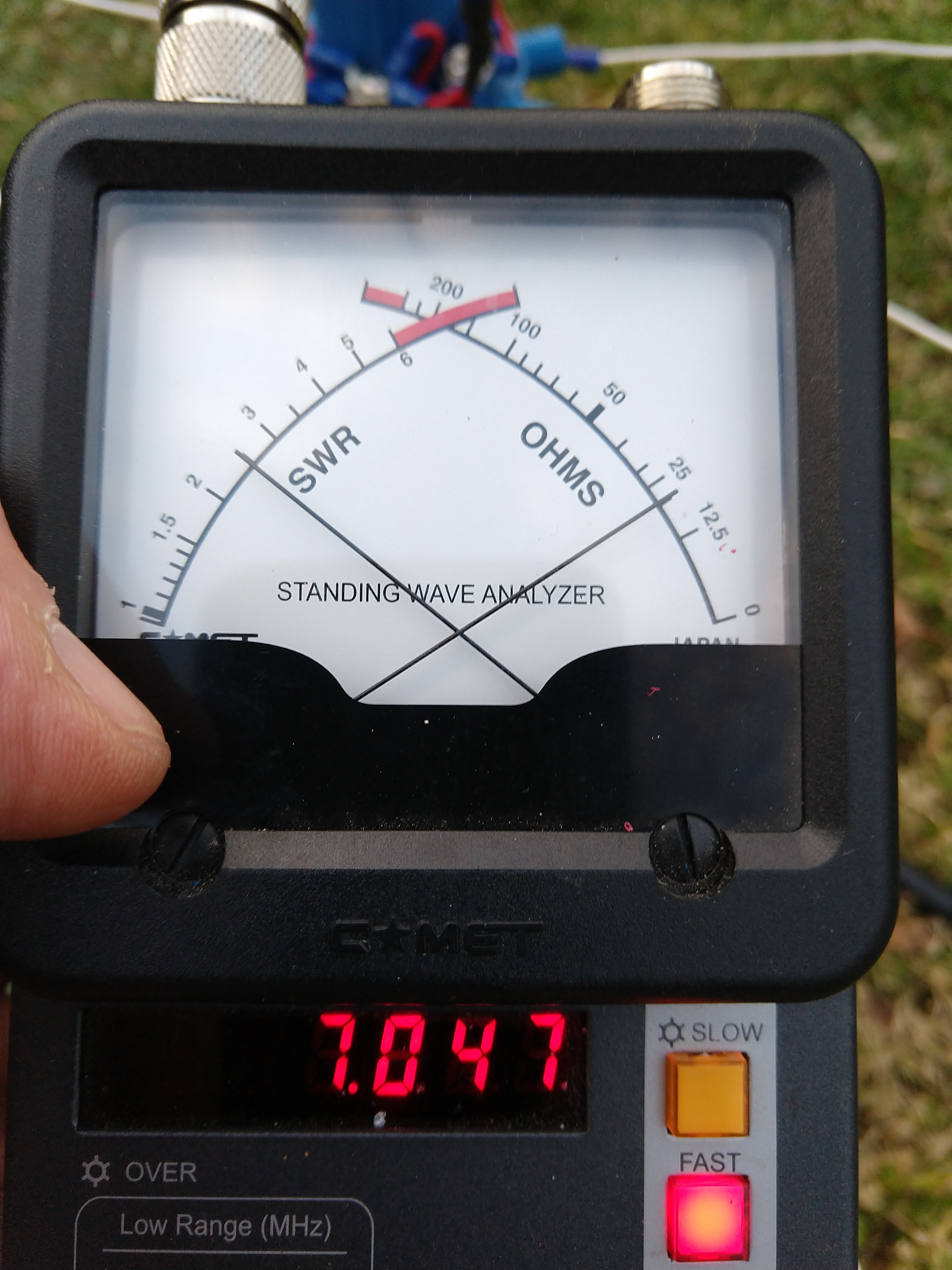
A resistive bridge type SWR meter doesn’t actually measure SWR – it measures impedance mismatch or impedance(however you want to look at it). SWR is calculated by the ratio of two volatges on the bridge. The SWR and impedance only relate correctly if the bridge impedance and feedline impedance are the same(50 ohms typically).  A resistive bridge works fine but you can do the same thing with  a simple resistive divider. When using a divider, you can use any value resistor you want(50 ohms in my design) and as long as you know the characteristic impedance of your feedline, you can correctly calculate the results with any feedline impedance (not just 50 ohm coax).By measuring three voltages across the divider(Vs, Vr and Vz), one can easily derive: total Impedance, resistive impedance, reactive impedance, SWR, and return loss. A resistive bridge is most accurate when mismatched, but the resistive divider is most accurate when match is optimal. So ask yourself would rather know more accurately what’s happening between SWRs of 1:1..to 2:1 or when it’s 3:1 or greater? The only drawback of this method is that you cannot determine the sign of reactance(capacitive or inductive) directly, but you can derive all of the magnitudes. This is because when you convert the voltages to DC values by means of diode detectors, all phase information is lost.

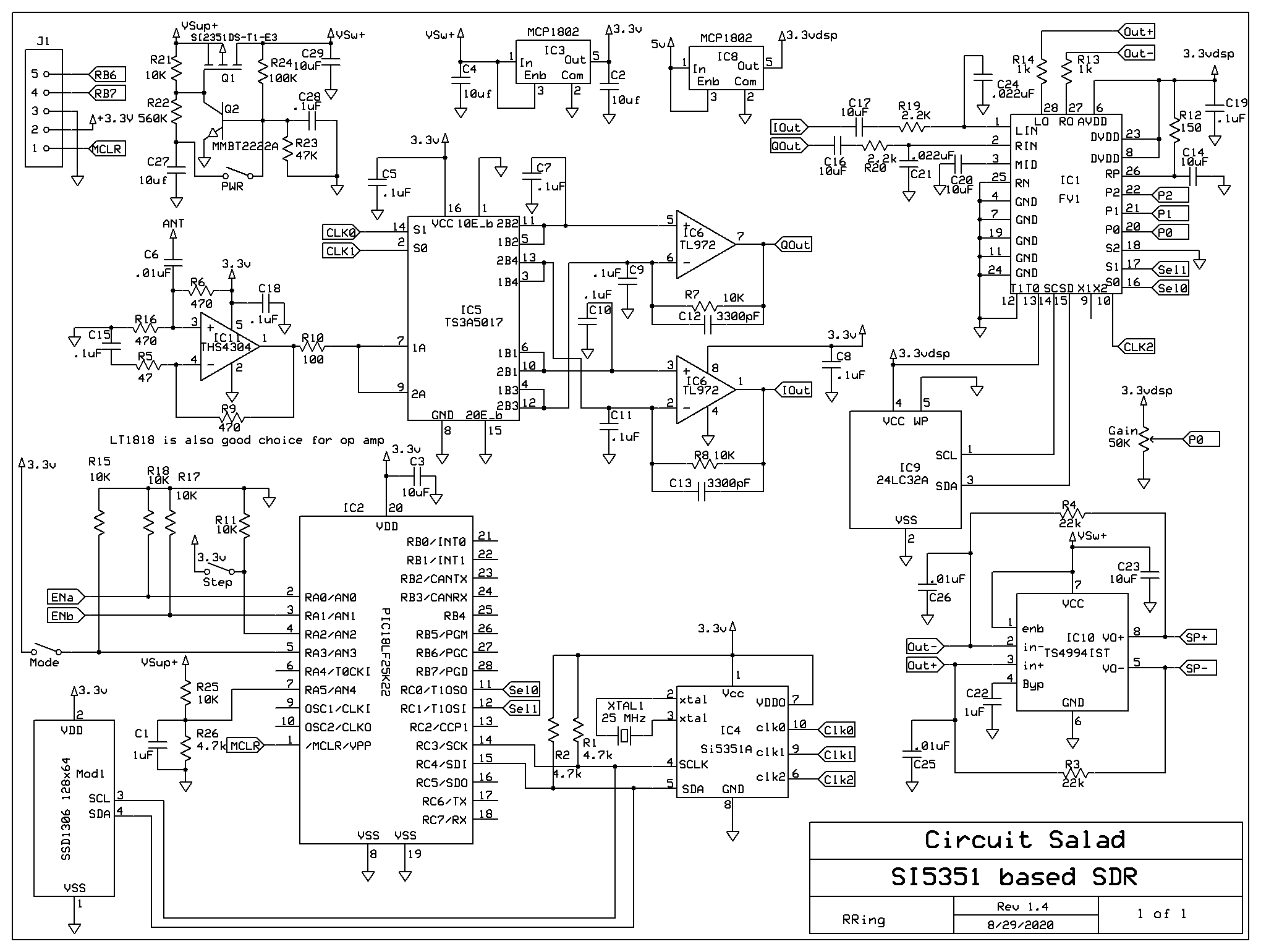
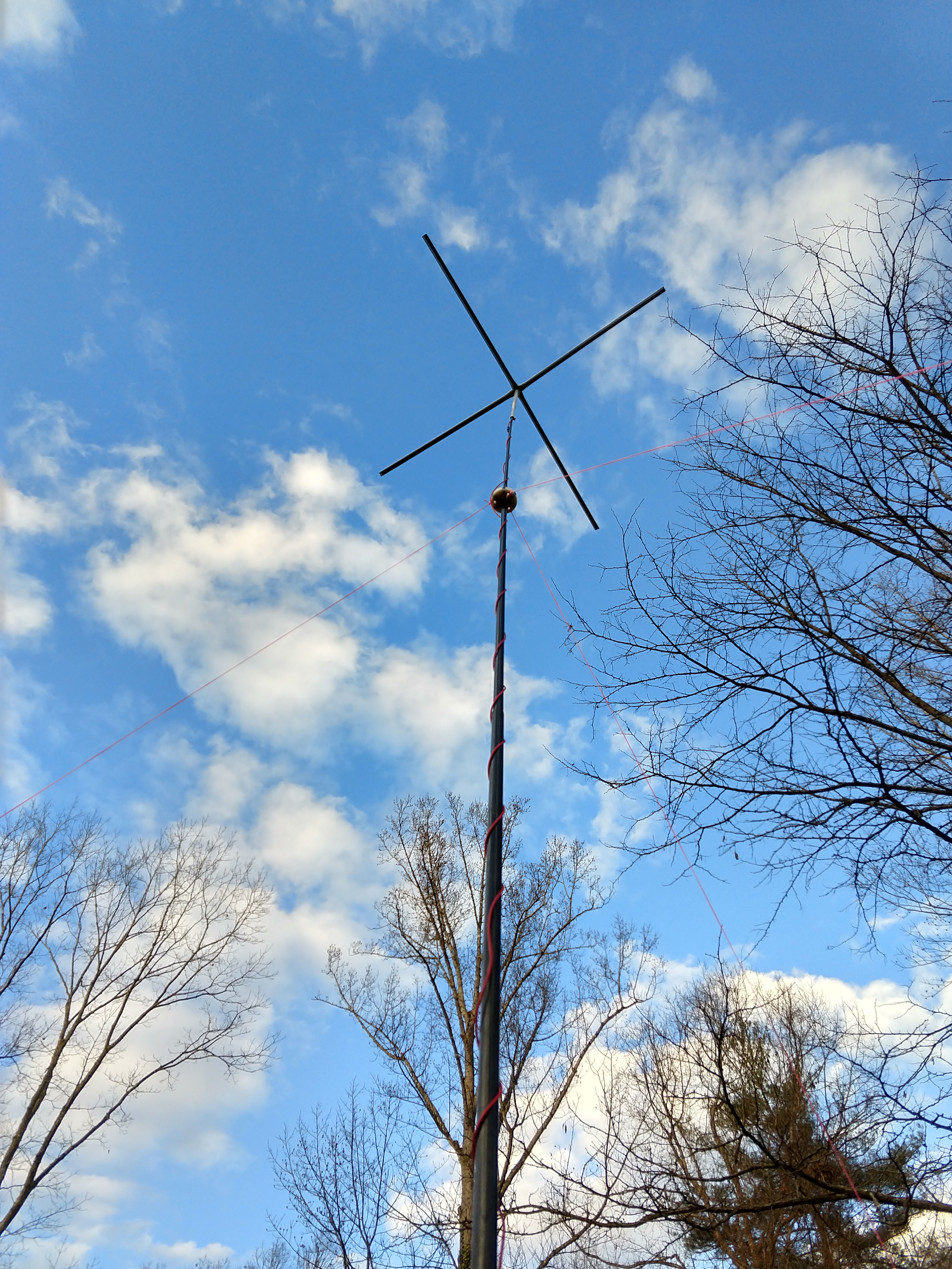
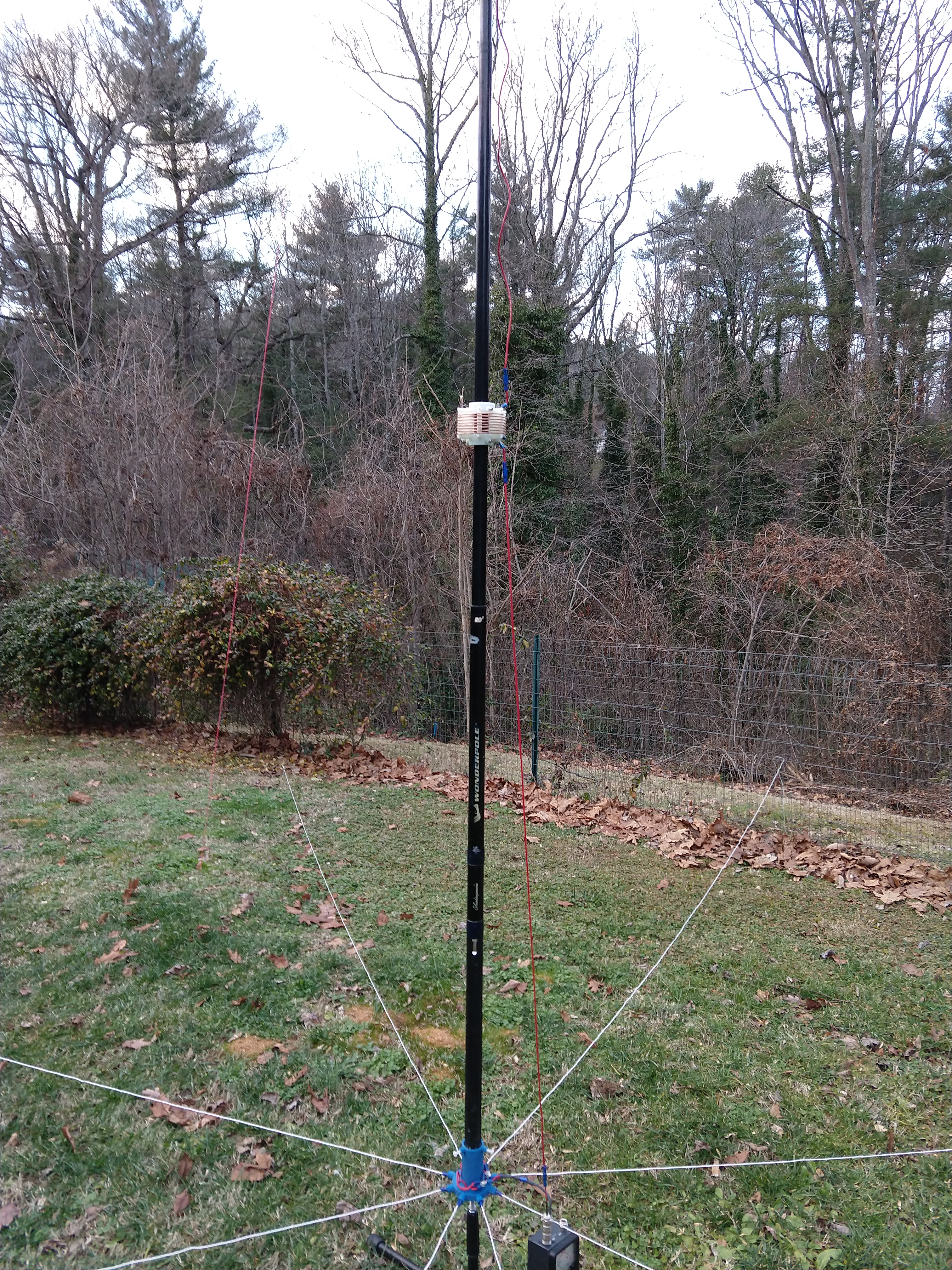
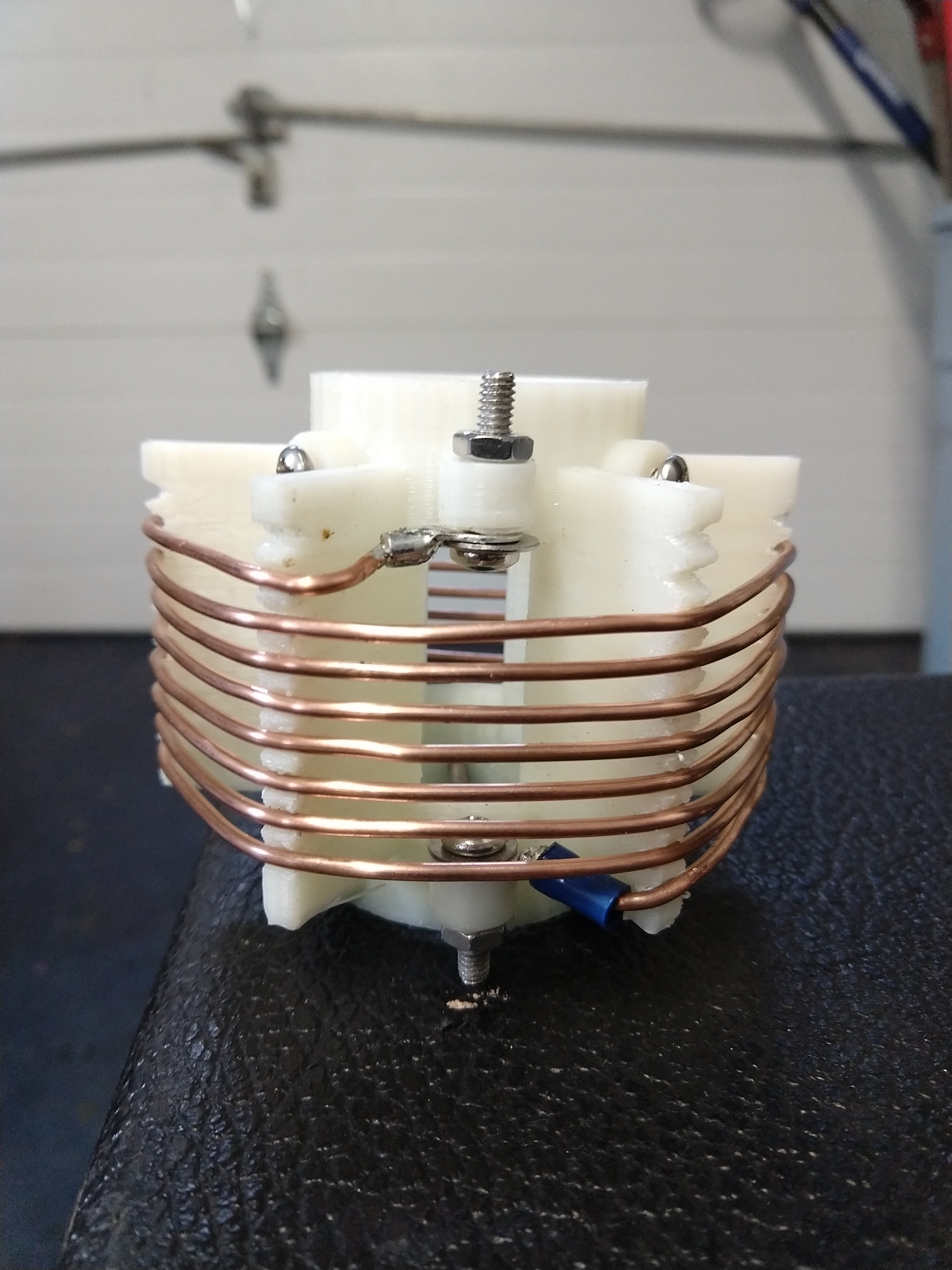
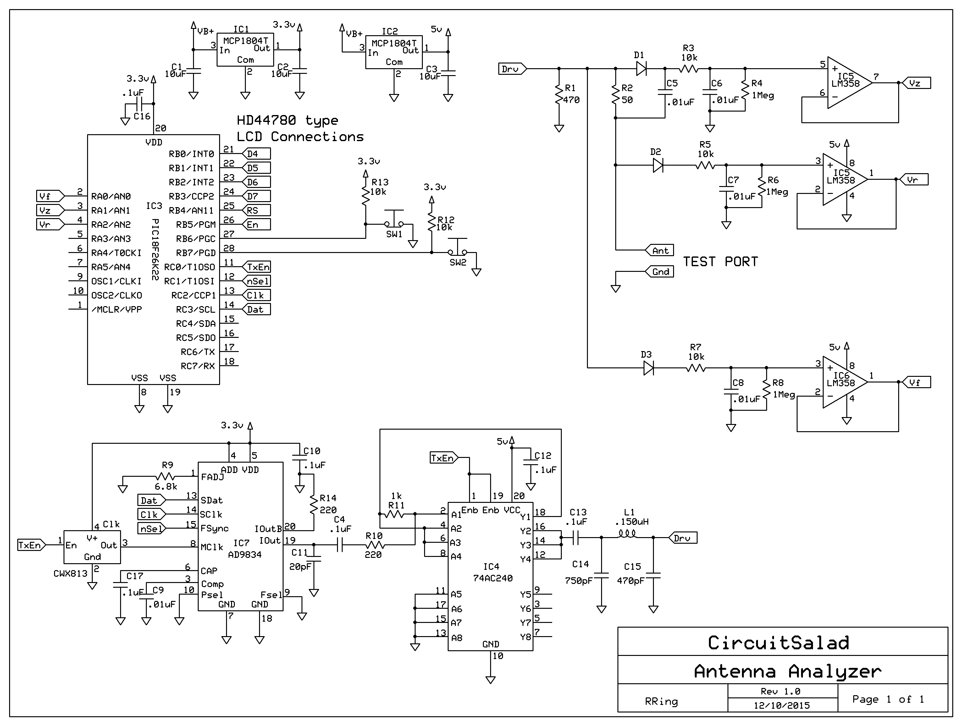
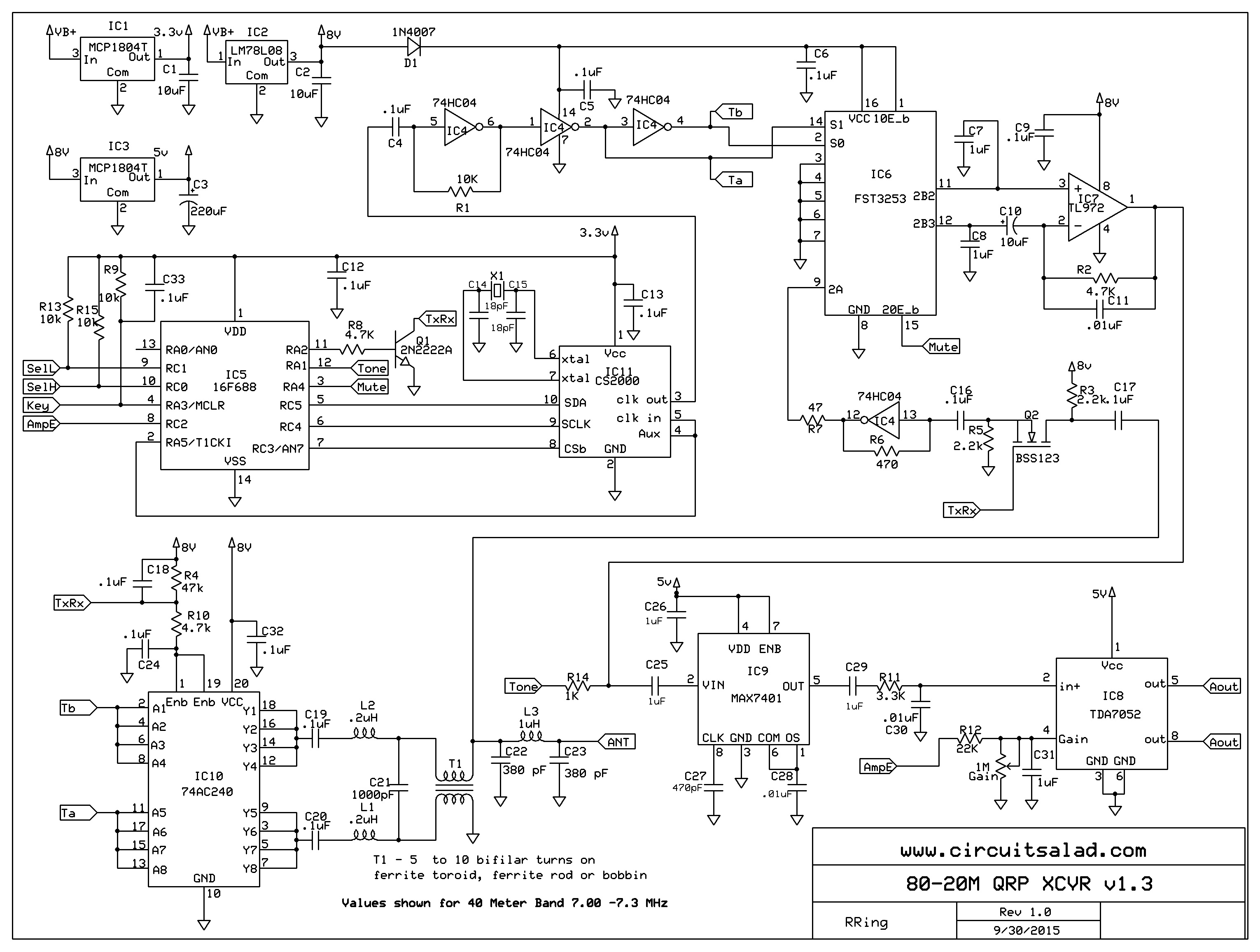
I decided to build a  small and reasonably simple antenna analyzer for 1 -30Mhz. I wanted it to provide accurate measurement of SWR, Total Z, R and X of the ANT.  Simplicity in operation and  moderate power consumption were also design goals. The schematic below is what I came up with.

Preliminary Schematic(not built yet)

Antenna Analyzer

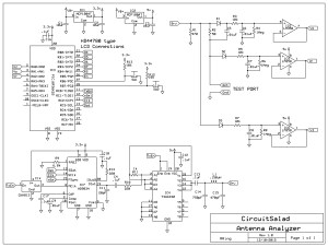
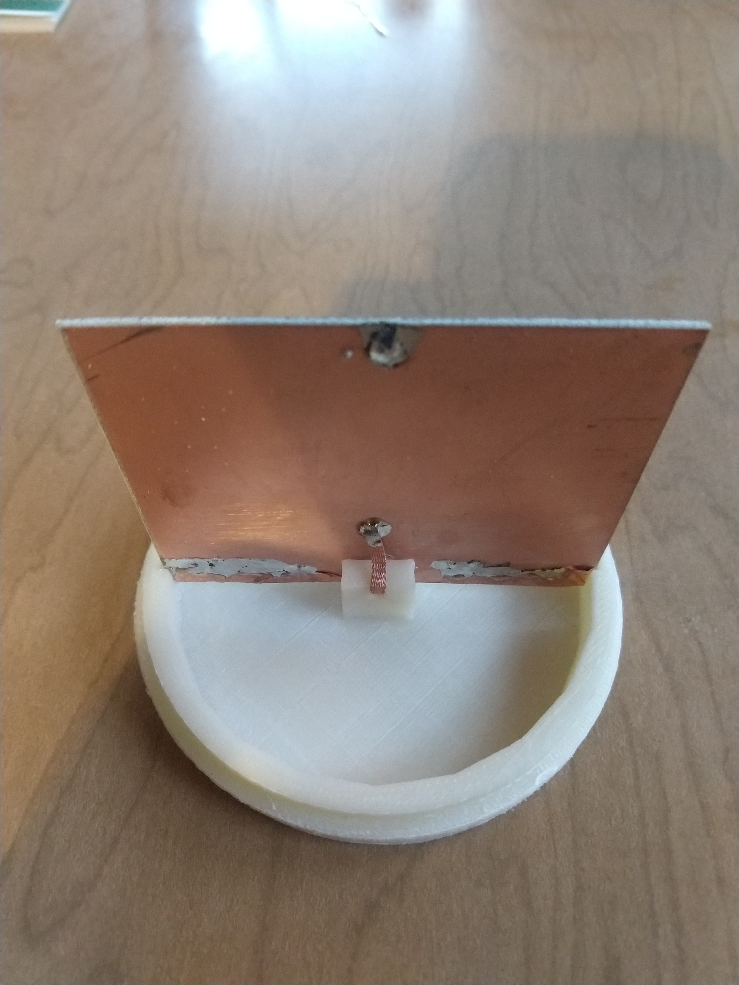
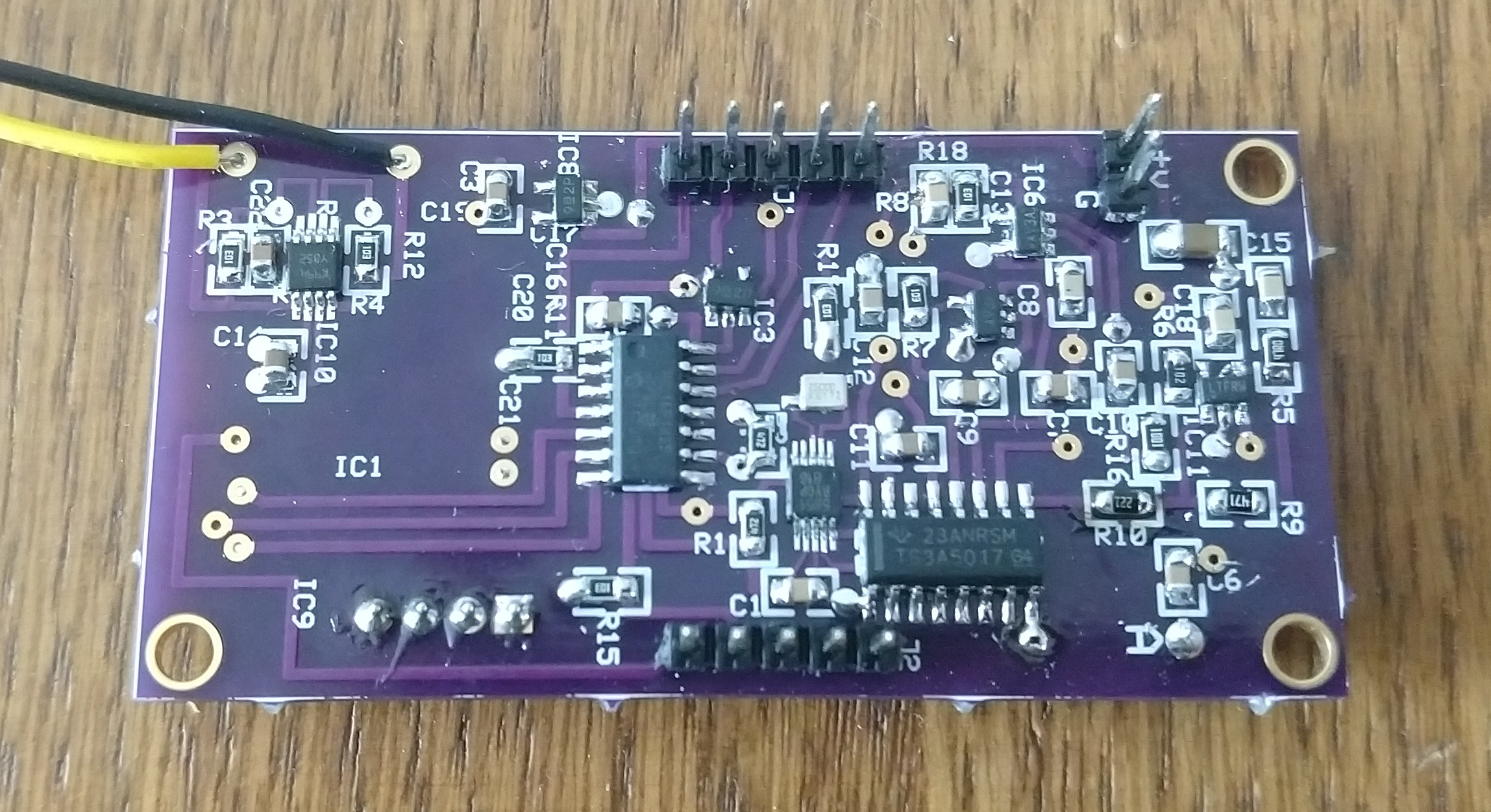
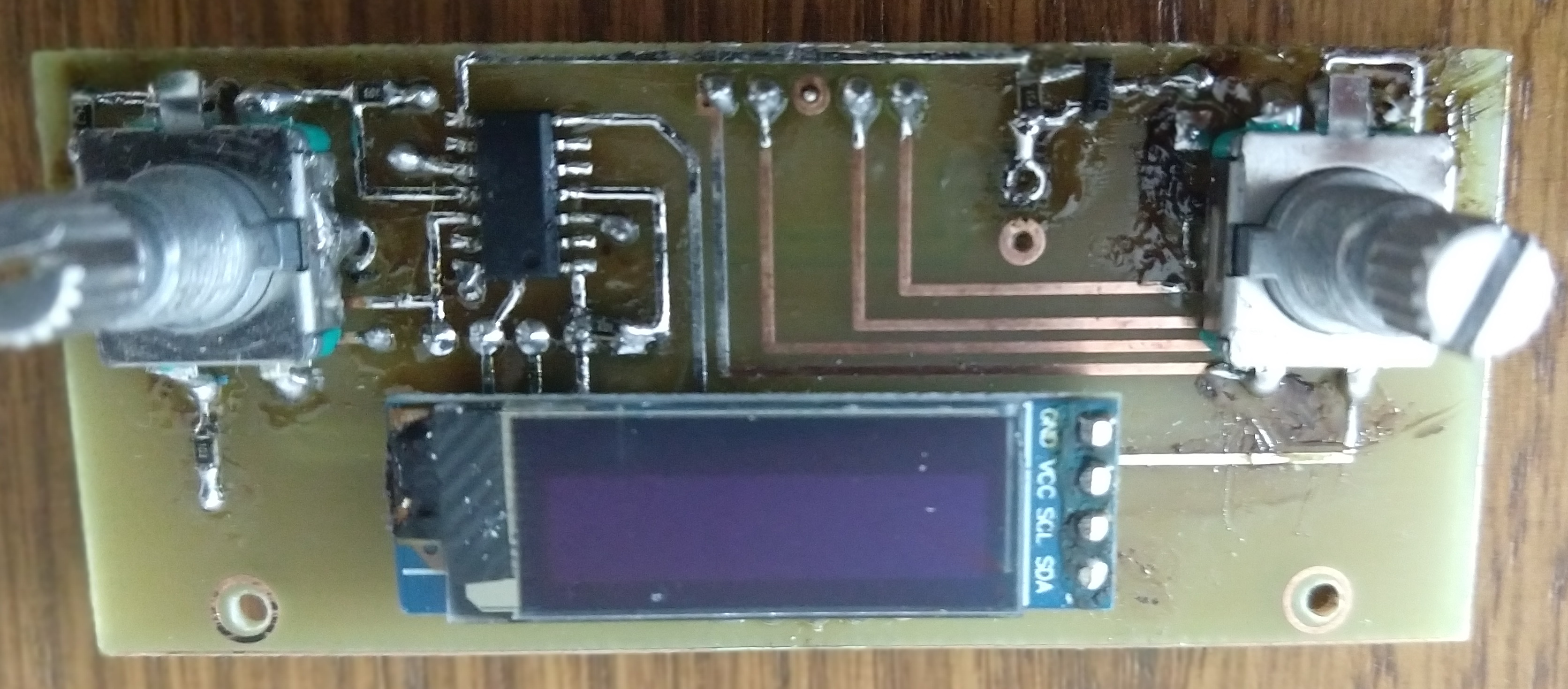
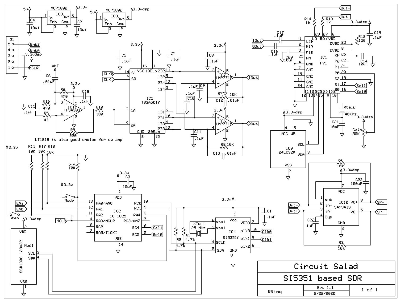
I have etched a circuit board and will build the analyzer in early 2016. I will update the post as I make progress. Expect some values in the schematic to change. Below is a discussion of the math required to derive all of the analyzer measurements. Vr requires a floating measurement, Vs and Vz are ground referenced.

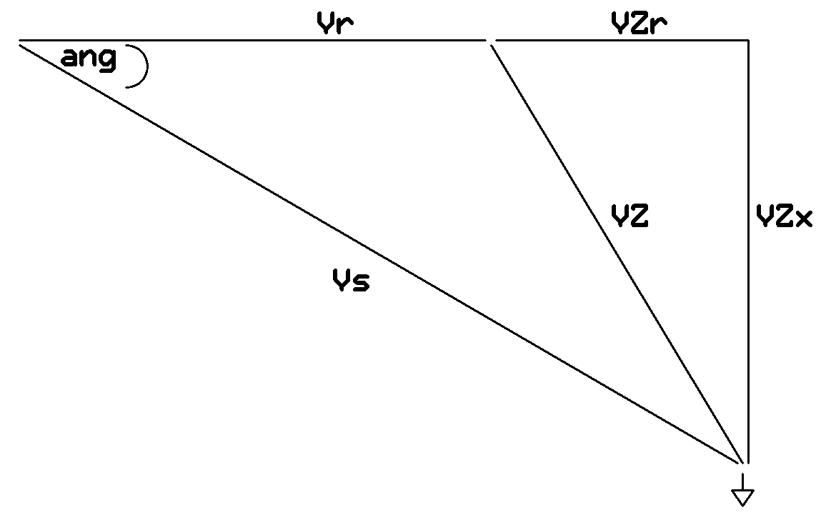
Diagrams for Analysis

example pic

Voltage dia

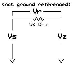
Using the Voltages Vs, Vr and Vz, one can create a triangle related to the classic power factor triangle where the hypotenuse(Vz) can be  seen to be shared and the cos(ang) allows one to find the reactive and real components of the impedance. One is required to find the cos(ang) using only the lengths of the sides of the Vz, Vr, Vs triangle. These values are the measured voltages from the diode peak detectors shown in the schematic. The law of cosines provides the solution.

cos(ang)  = (Vs²+Vr² – Vz²)/ (2* Vs* Vr)

Using node voltage equations, the following relationships can be derived from the simple divider shown above. Note that the triangle legs:Vs, Vr, VZ , VZr and VZx are synonymous with Zs, R, Z, Zr and Zx respectively

The total impedance seen across the signal source (Zs):  Zs = R*Vs/Vr

The absolute value of the complex impedance seen across the load connections of the resistive divider(Z): Z = R*Vz/Vr

The real part of the load impedance (Zr): Zr = Zs*cos(ang) – R

The complex part of the  load impedance (Zx): Zx = SQRT(Z² – Zr²)

With these equations we now have total load impedance Z, the resistive component Zr, and the magnitude(but not sign) of the reactive component Zx.

If we know  Zr and Zx, we can calculate the SWR and return loss as well:

First we calculate  Γ:  Γ = SQRT( (Zr-R)²+Zx²)/SQRT( (Zr+R)²+Zx²)

Now  SWR: SWR = 1+Γ/1-Γ   and return loss: return loss = -20 log Γ

Note: R used in Γ calculation is the characteristic impedance of the feedline not the R used in the divider (in my case they will be the same: 50 ohms).

QRP On Vacation

I used my new XCVR and my short portable dipole down in Ft Pierce Fl, over Thanksgiving.  The rig, antenna, feedline and tools all fit  in a camera bag and it was easy to setup. I made some 800- 1000 mile contacts on 1 watt and drank a few beers and smoked a stogie while doing it!

Short Dipole strung between two Palm Trees

IMG_20151128_102315719

QRP While Lounging Outside


40 meter XCVR size of an Business card with 1 Watt output, 7.000 to 7.150 MHz coverage

I tweaked my previous XCVR design to use push button tuning and made the board layout extremely compact. I improved the side tone injection to be absolutely  perfect – not too loud, full break in and no clicks. I went ahead and integrated my switch cap 8 pole CW filter. The schematic is fairly simple with 65 parts or so.. and the whole design fits into a 3D printed enclosure the size of an business card. The only penalty in the design is  signal on both side of zero beat(direct conversion). There is no AM leakage though and the filter rolloff is very good. The circuit is easy to build as it required no adjustment, or alignment, but uses some fine pitch surface mount parts requiring a very precise soldering station. When I got my boards in I literally just built it – applied power and starting using it. In this one I used a ferrite toroid for the Sorta-Balun, but I have used scrap bobbins from HF power inductor for this with great success . The push button tuning works well, it has freq (up/down) buttons which shift through at 10 Hz increments for 5 sec then goes to 1 Khz. It can run on a 10 to 24 volts supply. The 8 pole audio filter is adjustable to taste, by changing one capacitor(C27), and the side tone injection level with one resistor(R12). The choice of band only requires a firmware change and 3 inductors and three capacitors – which make up the RF matching filter. Its really a unique little transceiver. Its very small, reliable and has excellent performance. The TX frequency is offset 700Hz above receive frequency, but this could be made adjustable if desired(using the push buttons and the Key) – I just haven’t done it yet.

Schematic

QRPXcvrV3

The built XCVR

QRP UltraLite     QRP Ultralite2

I am going to provide a link to all the design files in the next few days including the 3D print files for the enclosure. I am also going to sell a couple units at cost(get rid my extra boards!) as partial kits( I will put most of the surface mount components on) and provide the switches and connectors that fit the enclosure (which I will also include). Will probably be around $70 for everything for a complete unit(except wire).

Link to design files:

https://www.adrive.com/public/j4AGQJ/HF%20XCVR.zip