A High Performance Regenerative Radio

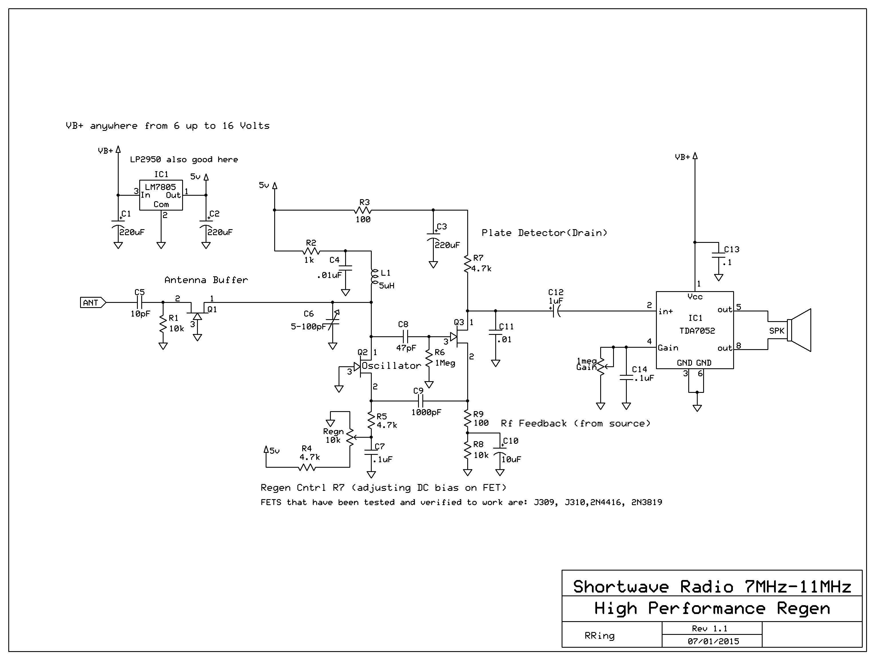
I have built countless regenerative radio circuits throughout the years and some have worked well – some haven’t. I was inspired by the circuit design of the TEN TEC regenerative radio kit. I used some of the same ideas, but changed the design to better match my design criteria. In this  design, I had eight important design objectives:

Simplicity – this type of radio should not be complicated and I have seen designs on the web that may perform well, but seem unnecessarily complicated.

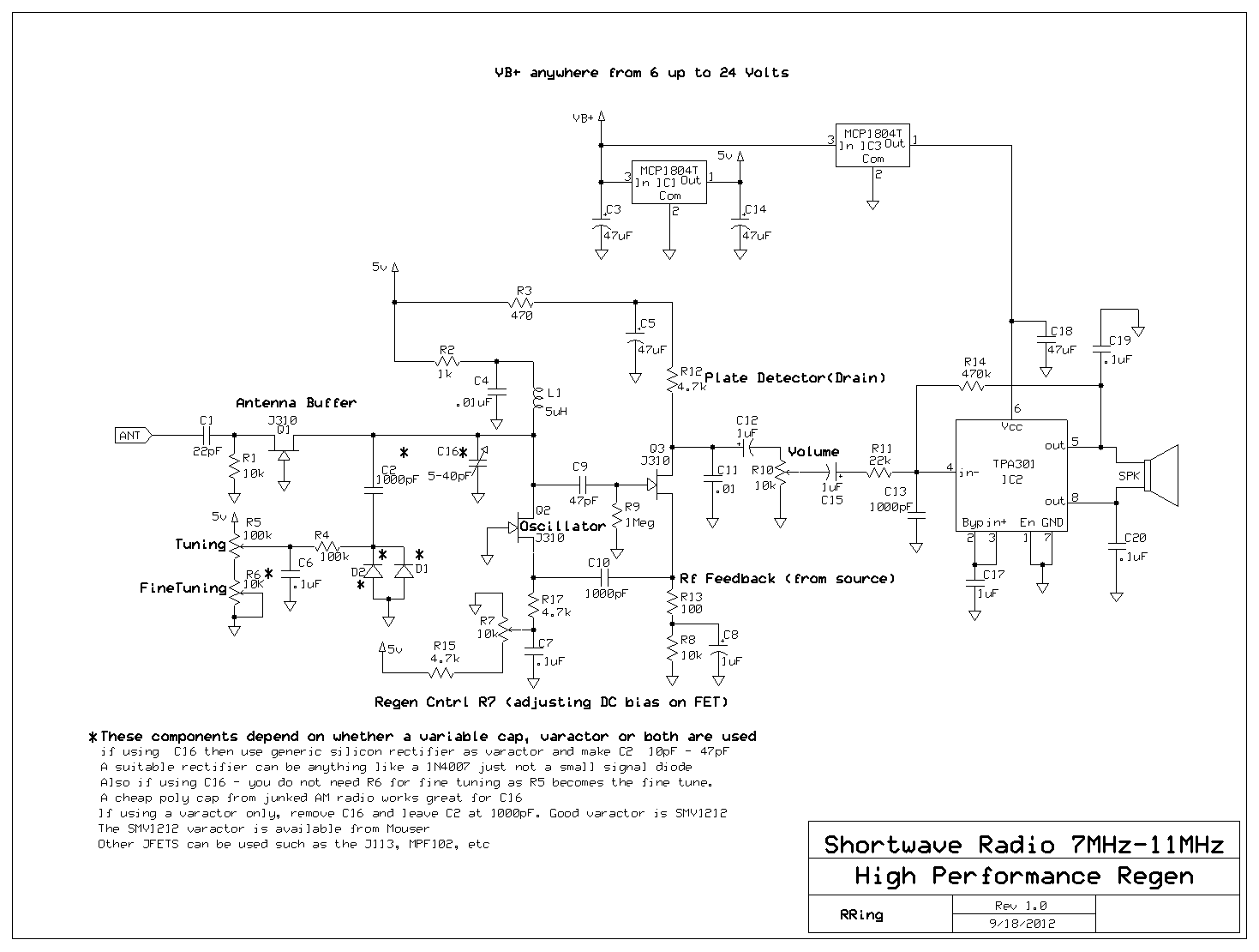
Tuning/fine tuning – I use a cheap poly variable for main tuning and a junk box rectifier as varactor for fine tuning.

No special inductor required – I have tried all sorts of junk box inductors and they all work great. With this design, no tapped coils or tickler windings are required. This design could easily be made into a multi-band radio

Extremely smooth and stable Regeneration control – I adjust a DC bias point condition instead of RF Feedback to control regeneration and the performance is excellent. There is no hysteresis or abrupt transition from regeneration to oscillation.

Ample Audio Gain with no motorboating or instability – I stayed away from the LM386(which could be used) and chose a TPA301 amplifier IC – which give excellent results.

Antenna Isolation – This is achieved with a simple grounded gate input stage which shares the LC tank with the oscillator.

Excellent sensitivity – This design is the best performing Regen I have ever built

No critical adjustments and easily repeatable results – I have built this circuit now three times with different inductors, for different bands and with different JFET device types on bread-boards, etc. The results have all been the same and I have only had to make minor tweaks to optimize performance for different JFET types and significantly higher or lower frequency bands. The radio currently tunes 7-11MHz.

The basic paradigm of this design is to break up the traditional oscillating detector into a separated regenerative amplifier and detector circuit.

The detector is  a “plate detector”, where RF is fed back to the Amplifier via a partially RF decoupled source(normally bypassed all the way for RF when used as a detector).

schematics:

Version 2: (07/30/2015)

regen_simple

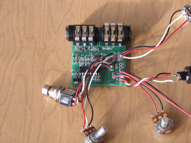
Link to PCB for version 2:(expresspcb format)

https://www.adrive.com/public/NPY7VM/Simple%20Regen.pcb

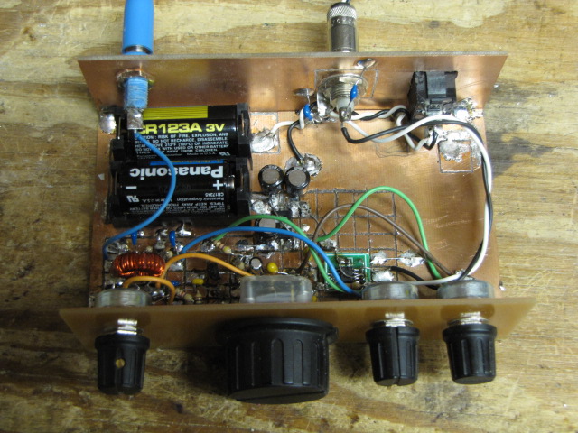
Version 1 (shown in video):

regen

picture of prototype:

IMG_5001

Video Demo:

Further Simplification of the Enhanced Orange Squeezer Compressor

It occurred to me that if one is willing to sacrifice some flexibility in the decay length of my compressor design; that it can be simplified by removing the source follower and the Zetex current sensor. What this means is that the control voltage is only half wave rectified instead of full wave, but if you just increase the filter cap – the circuit should still work fine. The trade-off is that you get limited to longer decay times only, but for most guitar applications this is fine. I have not verified this circuit but I will do this soon. I am confident it will work well. Removing these parts may make it more attractive to the DIY builder.

New Schematic:

https://circuitsaladdotcom.files.wordpress.com/2012/09/compressor3.gif

The miracle chip – the LT1144 charge pump

This IC is a switch cap charge pump the can source up to 50mA and can generate a negative supply from positve supply or can function as a voltage doubler. This thing is tough as nails and operates at 100KHz (easy to filter and above the audio range). It is over 90% efficient and requires two caps and maybe some diodes. I use it all the time for generation of dual supplies and doubled supplies for op amp circuits and high side nmos fet gate switching voltages. Check out the example circuits below. This IC solves all kinds of headaches with the addition of three or four parts to your circuit.

New Board layouts

I am going to do PCB board layouts of some of these projects in using expresspcb.com’s  free layout tool. I will use through hole parts as mush as possible. All the parts I spec will be available from digikey, mouser, mojo or small bear  – no condor eggs! I will post the files and anyone who wants can mod the boards or order them as is from expresspcb. It will take me a couple of weeks – I want to be very careful and make sure I have no errors.  So check back soon.

Pedal and Amp demo videos to be posted

I have been building a lot of guitar electronics these days … and more to come I hope! Having said that, I think it is important to show how they can be used in real music and how well DIY designs can perform as compared to commercial products. My first demo is of my portable busking amp and my FET discrete signal chain compressor. This demo  represents a classic jazz sound using the compressor to understate all of elaborate grips on the guitar and make the lines very smooth sounding even with heavy down strokes.

check it out at:

more demos to come shortly!

Here is a great tutorial on noise in Op Amp Circuits

This covers the basic equations for noise and more advanced analysis  but it distills down most of the analysis into good rules of thumb.

https://circuitsaladdotcom.files.wordpress.com/2012/09/noise-in-amps.pdf

The highlights include:

every 1K orf resistance adds 4nV/Hz noise.

noise adds as the sum of squares… so – larger sources dominate and large gain in the first stage minimizes noise contribution in later stages

Source impedance needs to be considered in  terms of its effect on op map current noise( often ignored)

When is A Capacitor not a Capacitor?

This is not a riddle but a painful reminder of  how un-ideal a capacitor can perform  in real world circuit conditions.  I measured the capacitance and Q factor for these capacitors shown below on a Agilent 4263B LCR meter, using 100Hz and 100Khz frequencies.

From left to right the capacitors in the picture are:

1000uF electrolytic,                     .01uF ceramic,                      10uF ceramic,                       .1uF tantalum

At 100Hz the results are as one might expect :   1007 uF, Q of 7     .014, Q of 100       8.6 uF , Q of 36       .104, Q of 80

The large electrolytic has a pretty low Q though indicating already at 100Hz its performance is starting to suffer

At 100Khz  things get really interesting : The 1000uF is now -.1 uF which is actually an inductor! The .01uF is .0098uF and the Q has gone down to 35. The nominal 10 uF(8.6) is now 8.2uF- not bad but the Q is down to 3. Finally the .1uF tantalum is now a .05uF with a Q of 1.2.

So even with this modest change in frequency, we can see capacitance starts to decrease as stray inductance becomes more of an effect. Also all of the capacitors start to become more lossy( low Q).

The bottom line here, especially with regard to decoupling, one large cap will not work well in most applications. One may have to use a combination of different type and value capacitors to achieve intended results.

PT2399 Design Updates

I have produced a PCB and built a new delay using the PCB and the original schematic. The results are gratifying. I did make a couple of minor adjustments.  The board is designed to fit in a 1590b stomp box. It draws 20mA so it works pretty well on a 9V battery.

R12 – changed from 33K to 39K

R2- changed from 56K to 47K

c19- changed from 2000pF to 2200pF

c16- from 247pF to 300pF

PCB Picture:

https://circuitsaladdotcom.files.wordpress.com/2012/09/img_4882.jpg

Video Demo Here:

Updated Schematic: