
Got a nice layout comming – hopefully some will be able to use it.
Month: October 2012
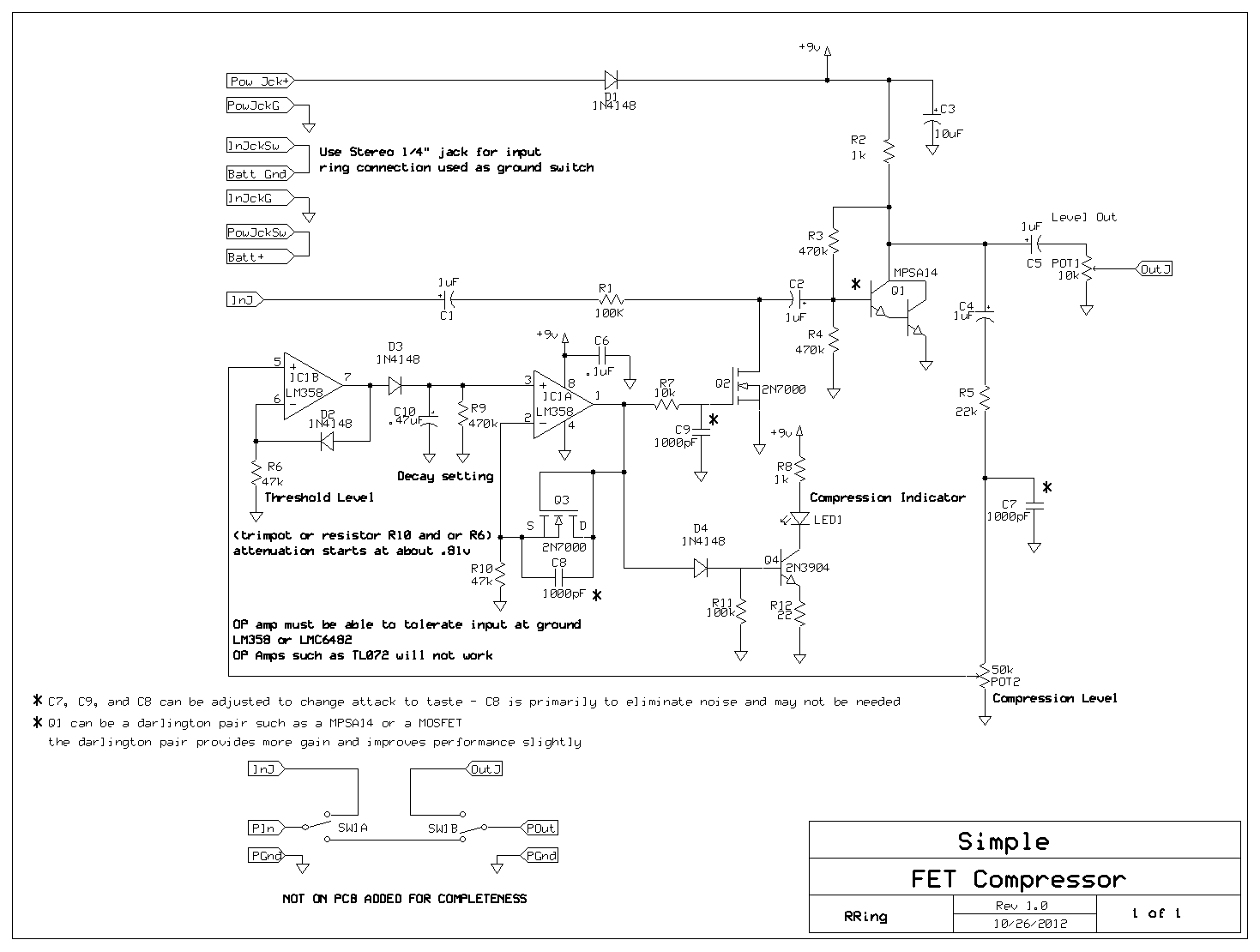
New compressor design – updated 10/28/12
Here is the schematic for a new compressor design, which has very small parts count but flexibility in threshold, attack and decay settings.
The design uses generic NMOS FETS such as the BS170 or 2N7000 and the only critical part is the one dual op amp which needs to tolerate voltage swing at or below ground. I am using a LMC6482 but others will work. Another designer built my original compressor using the LM358 and after looking at the data sheet believe it will work here as well.
I am using a 2N7000 as a voltage controlled resistor and it works well but cannot tolerate a drain to source voltage of even 100mV. I solve this by using shunt feedback from the drain to gate in the amplifier stage. This creates a cancelling signal at the input node, proportional to the gain, which reduces the net voltage seen across the 2N7000 down to tens of mV(with a 2 volt input).
The 2N7000 has turn on voltage starting at about .8 volts. The circuit has a 2N7000 configured as a supply independent voltage reference which provides the bias for the voltage controlled resistor. This reference is adjustable and can be used to set a variable threshold of compression or fixed at whatever threshold desired.
This design also uses a simple op amp peak detector which would be normally used in a sample and hold circuit. A bleeder resistor is added to create a decay response as desired. Because a peak detector such as this tracks instantaneous level changes – it needs to have it’s very abrupt shifting of output level smoothed out to eliminate sharp noisy spikes as the amplitude changes rapidly. This is achieved with a simple low pass integrator on the input of the 2N7000 voltage controlled resistor. This smoothing filter sets the attack. The peak detector can use just about any diode. I am using an LED which lights up and varies in intensity with respect to the amount of compression. This provides a visual indicator of how much compression is occurring. No adjustments are required to use different diodes.
In all, you can adjust the attack, decay, threshold, compression level (from 1:1 to greater than 3:1), and output level with this design, and it only uses three mosfets and one op amp.
Check out the schematic here: Consider this obsolete….. look below for improved design
https://circuitsalad.com/wp-content/uploads/2012/10/simple-compressor.gif
Update: I am changing the design of this compressor somewhat to eliminate some noise caused by the closed loop peak detector. The updated circuit is below. It uses an open loop compensated peak detector instead of the closed loop type. Also I separated out the compression level indicator – which really works well. It has the benefit of giving visual indication of threshold adjustments which can be set by R6 and R10.
I don’t need the final buffer either because the threshold settings and control loop gain allow the output match input level at max compression. Many of the component values can be adjusted so expect to play around with some values. Currently, I am using : R6(100k), R9(1Meg), R10(10k), C10(.1uF). Changing R9 and C10(smaller cap and larger resisitor) lets the op amp slew a little faster – no big deal. If I have any big revelations that something is better – I will post it!
New Schematic:
https://circuitsalad.com/wp-content/uploads/2012/11/mosfet-compressor1.gif
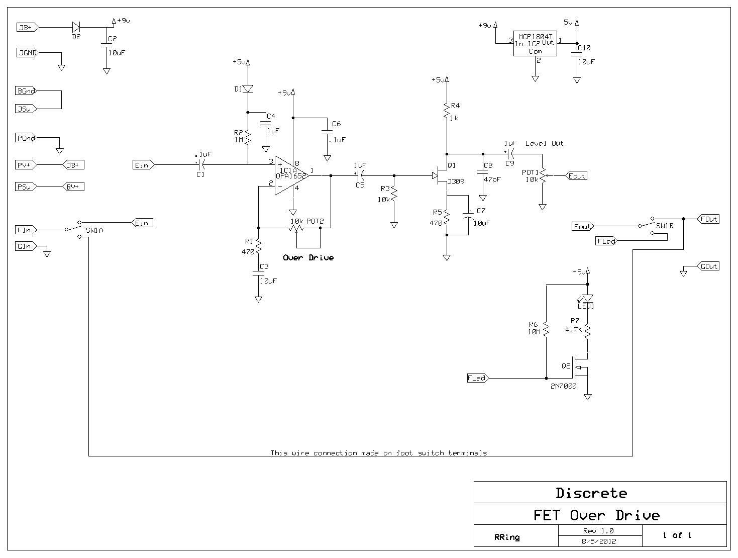
OPTO FET issue solved with Negative Feedback!
By applying shunt shunt feedback from the Drain to the Gate of the first JFET stage of my compressor, I reduce VDS across the optofet by a factor of 5! So with a input of 1 volt, the the VDS of the optofet is about 200mV worst case. Now it performs beautifully. The feedback consists of a 470k ohm resistor in series with a .1uF cap from drain to gate. Now the source must be bypassed with a 10uF cap – where before it was optional. The gain of the stage with this feedback is now about 4. What happens is that the feedback subtracts from the input at the optofet drain node greatly reducing the VDS across the voltage controlled resistor – while still providing gain.
Get the Simple FET distortion PCB layout here
Here is the simple FET distortion layout for through hole components. The schematic has minor changes to match this layout. So get this new schematic also. The layout is done with the expresspcb design tool. You can download their free CAD tool online. the layout can easily be modified or just ordered through expresspcb (lowest cost small quantity option is for 3 boards in three days for $60.00). The board is small and designed to easily fit in a 1590B box. I will add a parts list shortly.
Go to this link for .pcb file:
use slow download speed(free)
http://www.fileswap.com/dl/pPTjbxAOm/
new schematic:
https://circuitsalad.com/wp-content/uploads/2012/10/fet-overdrive_throughhole.gif
Another Demo of the REGEN
In this demo I have built the circuit with a crazy large 4″diameter tank inductor and used a SMV1212 varactor for tuning. There is no external antenna – just the tank coil. The circuit is built on a PCB proto board like the one posted for download only the parts are more tightly packed
check out the video:
http://www.youtube.com/watch?v=fE6UXi2yMYU&feature=player_detailpage
