Great App Note on Ceramic Capacitors

Below is a link to a tutorial on how bad ceramic capacitors are regarding holding their capacitance value under voltage bias. Basically the smaller the capacitor (physically) and the larger the voltage across it, the less the actual capacitance will be. I have always know this to be true but I didn’t realize it was as bad as describe below. This was a good reality check for me to make sure and select capacitors for a design carefully!

https://www.maximintegrated.com/en/app-notes/index.mvp/id/5527

Improved Power Toggle Latching Circuit

Awhile ago, I posted an example of a Power toggle circuit using a handful of components that I  use all the time to allow a momentary switch to control Power On/Off function.

https://circuitsalad.com/2014/04/12/simple-momentary-switch-latching-circuit/

The circuit works well but can require a series diode with the output to prevent  stored charge or magnetic energy from re-energizing the lating function such that it won’t turn off. The diode drop may be undesirable, so I modified the the circuit  as show  below.

Alternate Power Toggle

The addition of R7 and C8 eliminates this problem in every circuit I have tried and is sure-fire in reliability. Normally, C8 can be omitted, but I added for one application with very strong RF fields near by.  As before, the circuit draws no current when off and can toggle within a second or so.

Of course you might ask why not just use a toggle switch?  Well of course you can but you can get momentary switches cheaper, they can be much smaller and generally I find switch bats ( toggle levers) to be un- aesthetic and sometimes cumbersome. So now I usually do something like this.

Simple Momentary Switch Latching Circuit

I had to cook up a quick circuit to allow a momentary switch to turn the power on and off for a circuit but draw no current when off. I came up with this. I am sure someone else has done something similar before, but it was fun figuring it out for myself.

It uses two transistors or a transistor and a PMOS FET. It can be tailored to work with a large range of voltages… and very low voltages when using the NPN/PNP version. The values shown work well from about 5 volts up to 12 volts. If the  voltage is higher than that, some of the resistors (R1 and R5) should be increased so that the on current used by the circuit is not excessive.

I noticed when you have highly reactive inductive or capacitive loads the circuit can fail to turn off. You can use either an isolated switching element or a blocking diode to solve this.

It works because in the initial state the PMOS is turned off and C1/R4 is charged up enough to turn on the NPN. When the switch is pressed, the charge on C1 biases on the NPN, which then turns on the PMOS. Once the PMOS is on, R3 biases on the NPN, latching the “on state” for the circuit. However now the collector of Q2 is a path to ground and C1  discharges to ground through R2(R4 also). Now, if the switch is pressed the NPN gets turned off long enough to shut the whole thing off again.

You can adjust the resistor values and the C1 value to adjust the response time, quiescent “on” current, etc. I advise building it as shown, using  a 9V battery  and a LED as a load, to get a feel for how it works before changing the values too much. The values are interrelated… so you can’t make extreme changes to one component value without adjusting others.

momentary latching circuit

The miracle chip – the LT1144 charge pump

This IC is a switch cap charge pump the can source up to 50mA and can generate a negative supply from positve supply or can function as a voltage doubler. This thing is tough as nails and operates at 100KHz (easy to filter and above the audio range). It is over 90% efficient and requires two caps and maybe some diodes. I use it all the time for generation of dual supplies and doubled supplies for op amp circuits and high side nmos fet gate switching voltages. Check out the example circuits below. This IC solves all kinds of headaches with the addition of three or four parts to your circuit.

Here is a great tutorial on noise in Op Amp Circuits

This covers the basic equations for noise and more advanced analysis  but it distills down most of the analysis into good rules of thumb.

https://circuitsaladdotcom.files.wordpress.com/2012/09/noise-in-amps.pdf

The highlights include:

every 1K orf resistance adds 4nV/Hz noise.

noise adds as the sum of squares… so – larger sources dominate and large gain in the first stage minimizes noise contribution in later stages

Source impedance needs to be considered in  terms of its effect on op map current noise( often ignored)

When is A Capacitor not a Capacitor?

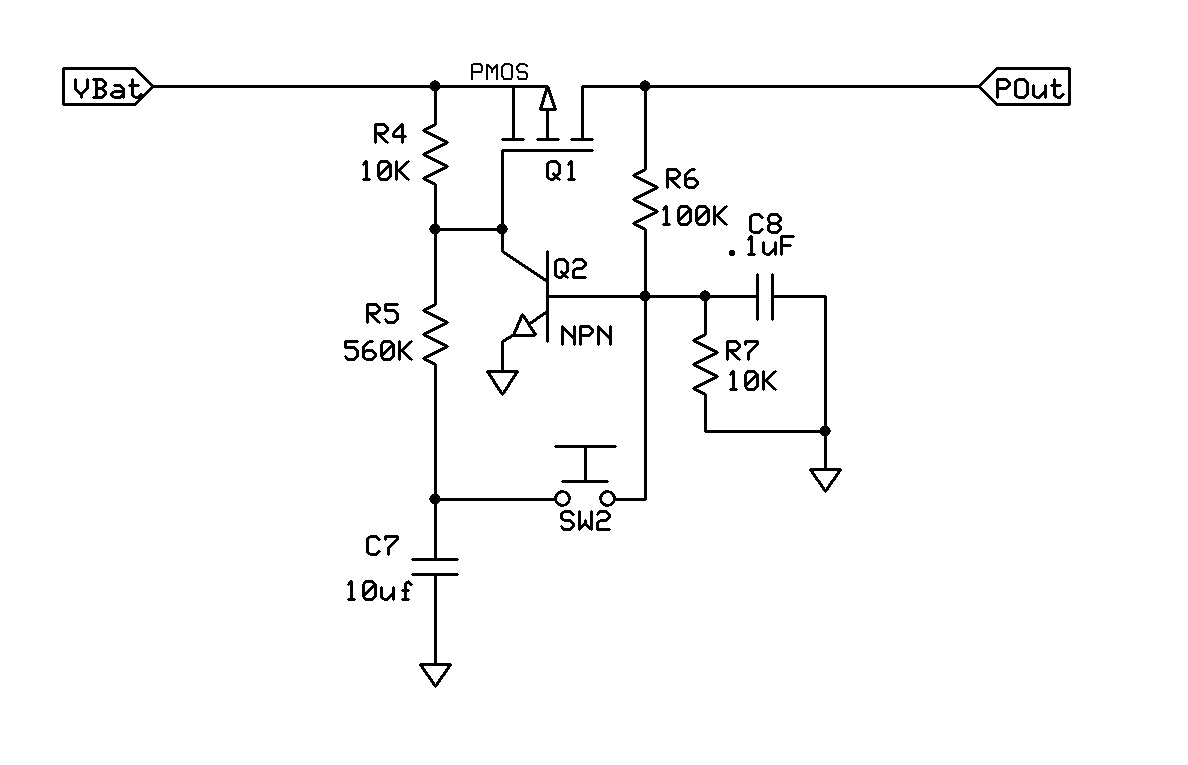
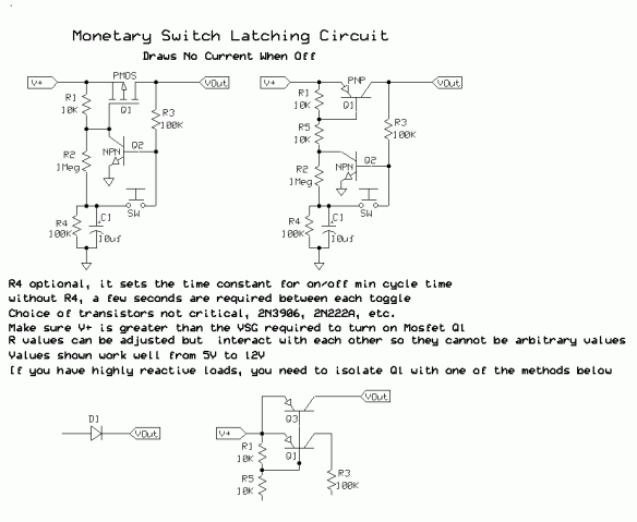
This is not a riddle but a painful reminder of  how un-ideal a capacitor can perform  in real world circuit conditions.  I measured the capacitance and Q factor for these capacitors shown below on a Agilent 4263B LCR meter, using 100Hz and 100Khz frequencies.

From left to right the capacitors in the picture are:

1000uF electrolytic,                     .01uF ceramic,                      10uF ceramic,                       .1uF tantalum

At 100Hz the results are as one might expect :   1007 uF, Q of 7     .014, Q of 100       8.6 uF , Q of 36       .104, Q of 80

The large electrolytic has a pretty low Q though indicating already at 100Hz its performance is starting to suffer

At 100Khz  things get really interesting : The 1000uF is now -.1 uF which is actually an inductor! The .01uF is .0098uF and the Q has gone down to 35. The nominal 10 uF(8.6) is now 8.2uF- not bad but the Q is down to 3. Finally the .1uF tantalum is now a .05uF with a Q of 1.2.

So even with this modest change in frequency, we can see capacitance starts to decrease as stray inductance becomes more of an effect. Also all of the capacitors start to become more lossy( low Q).

The bottom line here, especially with regard to decoupling, one large cap will not work well in most applications. One may have to use a combination of different type and value capacitors to achieve intended results.

Using A PMOS FET as Reverse Polarity Protection

I fry a lot of electronics – so I like to include reverse polarity protection when I can. But there is a problem with using a traditional silicon diode, namely dropping .7 volts across the diode(more with high current). Consider that in an earlier post I described a 20 watt,  amp I designed. If this amplifier is drawing 1 amp, a standard silicon diode wastes .7 Watts or more!

A better choice is to use a PMOS FET as shown in the picture below:


The way it works is that the Gate is grounded and only when the SOURCE is at a higher potential than the GATE will the PMOS conduct across from Drain to Source. This only occurs when the supply voltage conducts across the internal substrate diode(Dinternal), energizing the SOURCE and allowing conduction. When the PMOS is turned on, the drop across the mosfet is only millivolts (depending on the mosfet specs), much less than a traditional diode.