Go here for the most up to date circuit /firmware mods: Design Updates
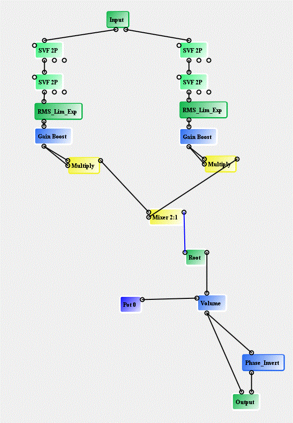
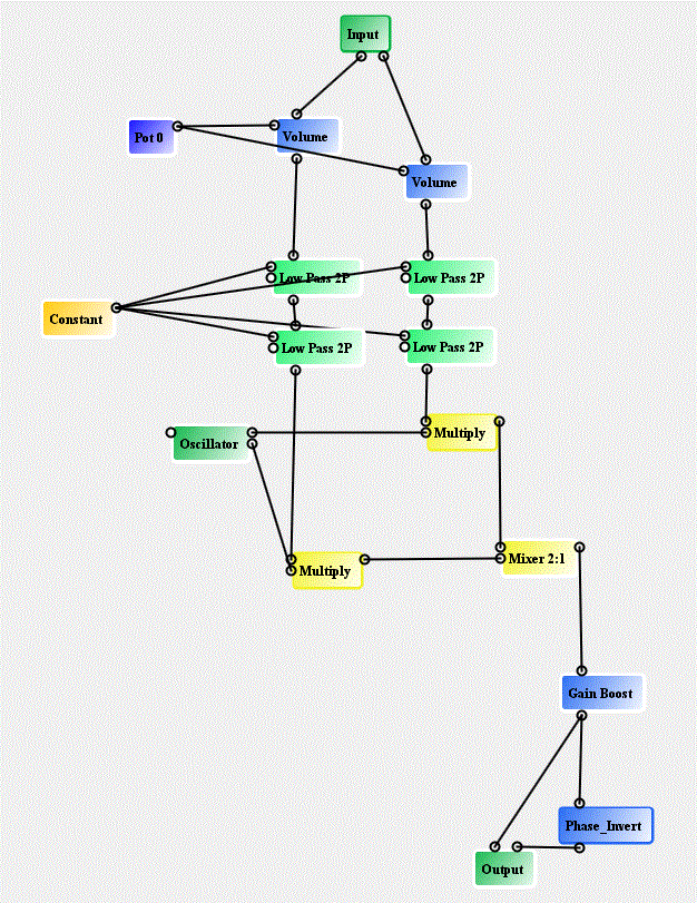
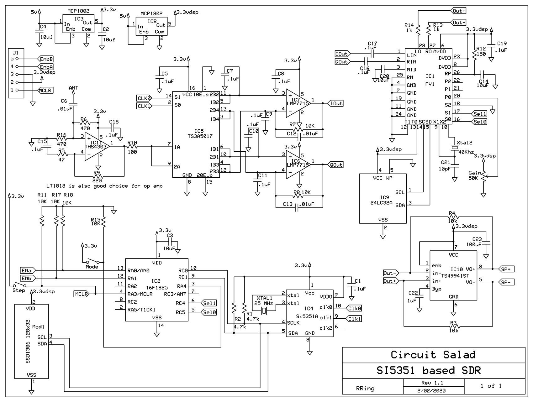
This is a revised version of my FV-1 based SDR. I replaced the CS2100 clk generator with the Si5351 clk generator. The Si5351 has some advantages over the CS2100, namely you can generate quadrature clks directly. This simplifies the hardware design and improves the quadrature accuracy. The sideband rejection in LSB/USB modes is impressive..somewhere around 60 db as best I can measure. The DSP processing is accomplished by the use of a FV-1 audio processor. The device makes the base band signal processing a snap. It requires some code to be loaded on a EEprom but the circuitry is simple and allows for up to 8 selectable programs. I created three: AM/USB/LSB . The FV-1 provides for three analog POT inputs to control any parameters you choose. Gain, variable filter bandwidth and depth, AGC are some examples of adjustable parameters if you desire. I kept it simple and created fixed band pass filters to taste. I did use one of the controls for AF gain. The design has no tuned circuits or band pass filters but they could easily be added. It works just fine without them. Occasionally, I come across a ghost signal from harmonic mixing, when tuning, but not enough to matter. The design uses an OLED display and a rotary encoder for tuning. The frequency coverage is from 2.7 Mhz to 25Mhz. The bottom limit is created by the inability of the Si5351 to support quadrature below this frequency. Although I have improved my DSP programs for the FV-1 and have developed new display drivers and the new code for the Si5351, useful detail about using the Fv-1 can be found in my original design from a few years ago: https://circuitsalad.com/2015/06/19/comming-soon-stand-alone-software-defined-radio-baseband-demodulator-no-computer-required/
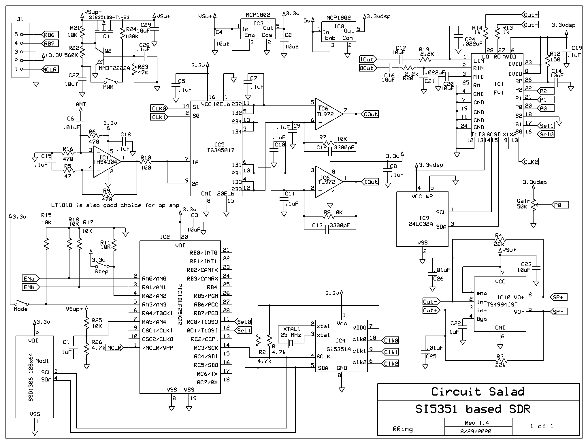
Schematic: Updated 05/17/2020

The design uses a LT1818 or THS4304 low noise op amp as an RF input with gain. It provides a constant and reliable resistive Rf termination for the sampling detector. This allows for random antennas to be used without adversely affecting the input termination to the detector. All the code to operate the main processor(display/clk generator/tuning, band select and receive mode) was written in MikroC which is a C compiler for PIC and AVR processors. The generation of quadrature signals out of the Si5351 is not difficult to implement once you know how but..figuring that out took me a couple weeks of experimentation! You can connect switches, the encoder, volume pot and display directly to the main board for operation but I created a secondary board to mount the display and encoders. Instead of an analog pot and selection momentary switches, I used another microcontroller and two encoders(with one built in momentary push switch each) to create all of the switching signals, gain control, etc. This allowed me to have just two controls for all features. The controls include: tuning, audio gain, mode, and tuning step. Tuning resolution is from 1Hz to 100KHz . For fun, I made the output of the FV-1 differential into the audio amp. This is not necessary.
Here is a link to all the files used to build this radio in a zip file(updated 2/07/20):
Tech File Download
The schematic and PCB was done with express pcb freeware. The C compiler used was MikroC, and FV-1 assemble was built in SpinAsm which is free and available from Spin Semiconductor(who makes the Fv-1). The gerber files provided were created for OSH park. I had my boards etched by them. If anyone is interested in building this radio or leveraging elements of the design. I can answer questions.
Misc Notes: I use a 16650 3.7v lithium rechargeable battery to power the radio. The current draw is about 100 mA with audio. The radio works even when the regulators drop out so it will work at 3 v.
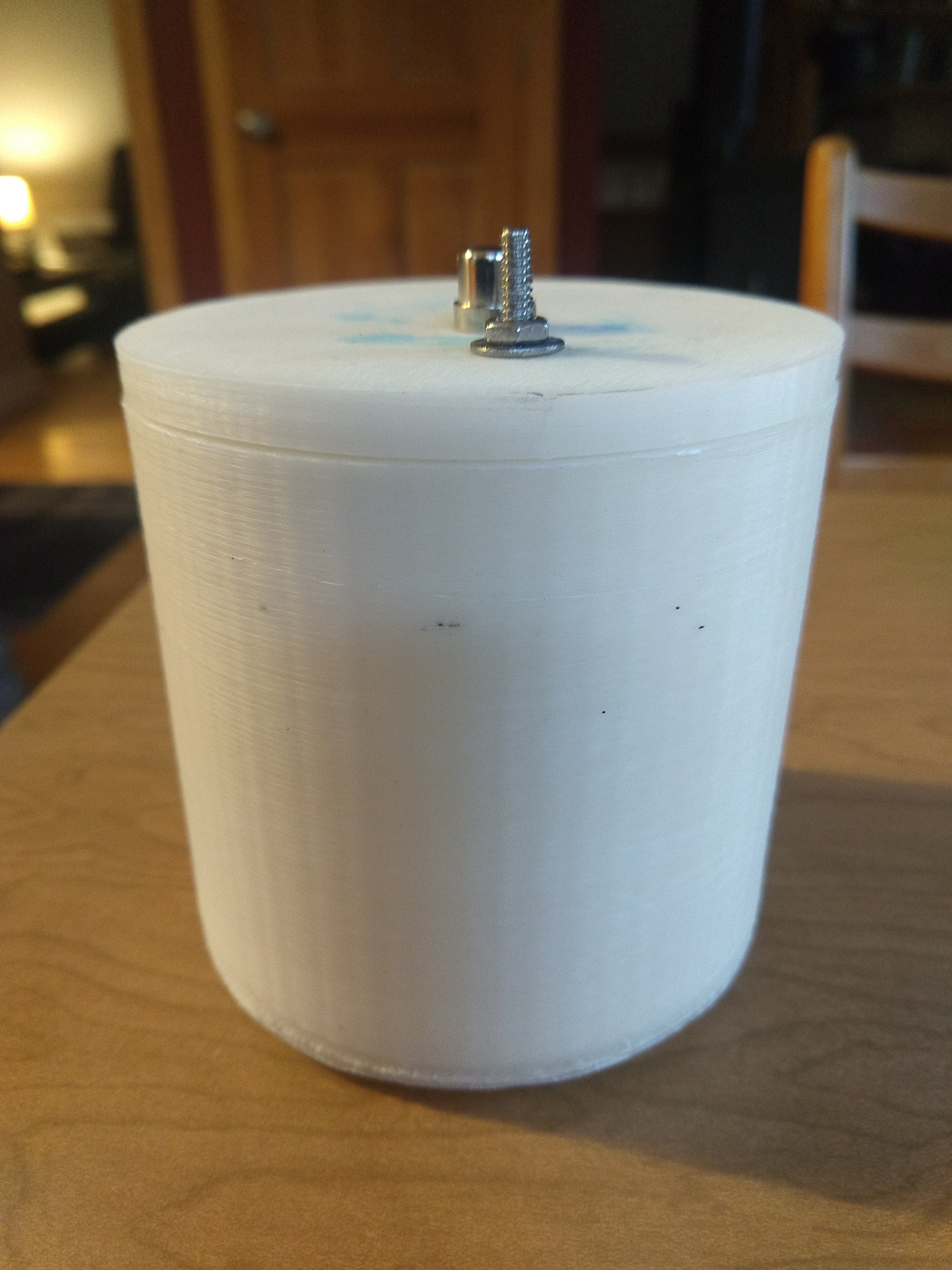
The enclosure is a machined aluminum 1590A style hammond box which you can buy on Ebay from alpinetech. They are $14.00 which is pricey but they are not cast. The quality is much nicer and you can anodize them. It’s a different topic but home anodizing of aluminum is easy…and I do it with all my enclosures now. In this example, I anodized twice to create the base blue color and then the labeling as well. It looks really clean with this method. The nice thing about anodizing is if you make a mistake, it’s really easy to go back and redo the process.
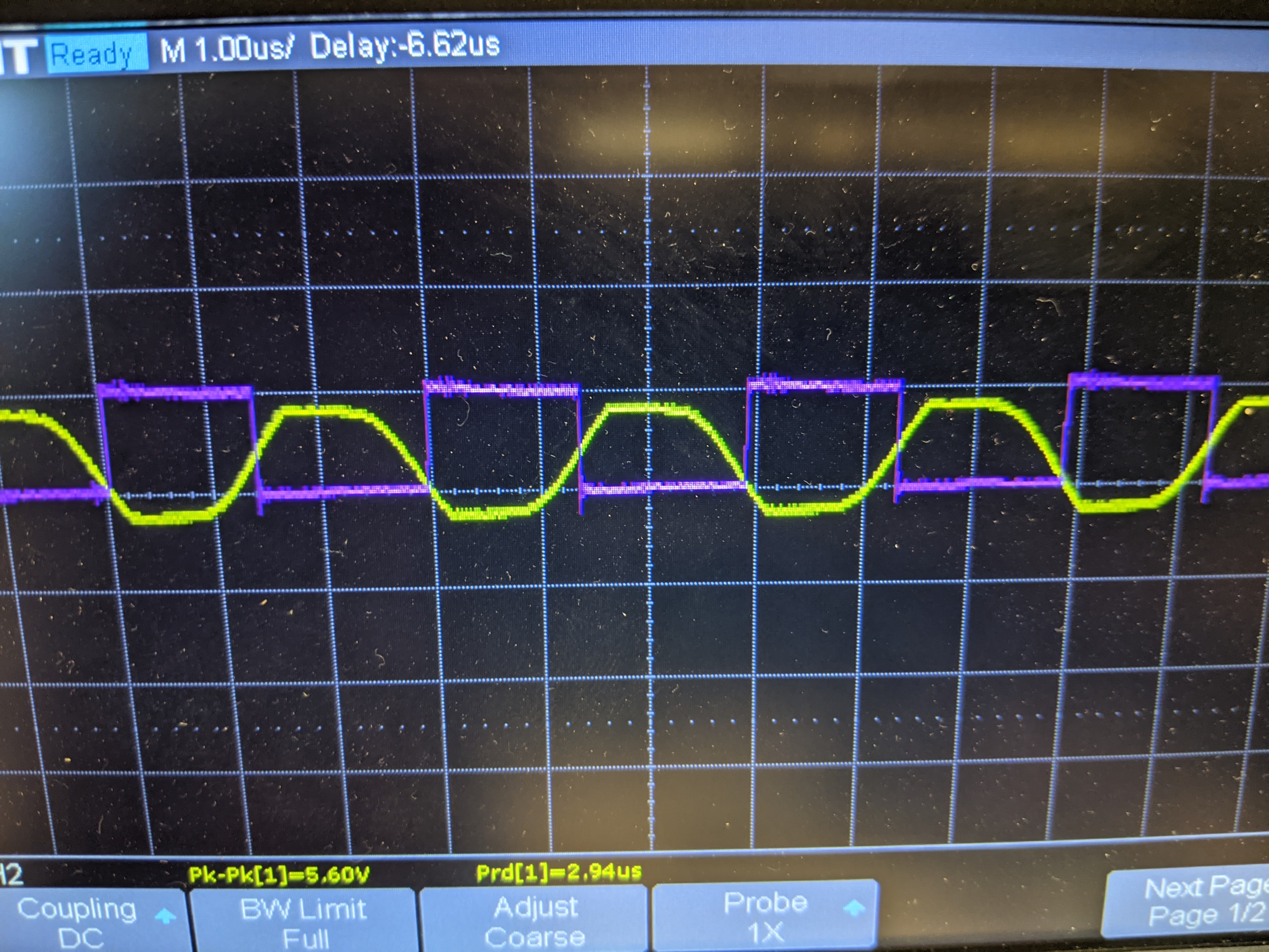
Designers will note that the resistive terminations on the input RF OP amp contributes to the noise figure of the radio. As a practical matter. a negative impact on performance is not noticeable because of atmospheric noise in the shortwave bands. For the best performance…no front end circuitry or a different front end input amplifier should be considered. Note that the op amp serves to bias the analog switches to half supply; so this bias must be provided to the sampling detector if the input termination is modified. R10 set the impedance of the sampling detector, conversion gain, and low pass roll off. The schematic shows a value 0f 210 ohms…I think I am using 100 ohms actually now…which works well.
If you want quadrature out of the Si5351 below 3MHz you can create two outputs with 0 deg offset with one output at F and the other at 2F. You can then drive an analog mux with those signals and generate quadrature sampling for low frequency applications. Just note the output sequence of the samples change so you have to flip two outputs of the detector.
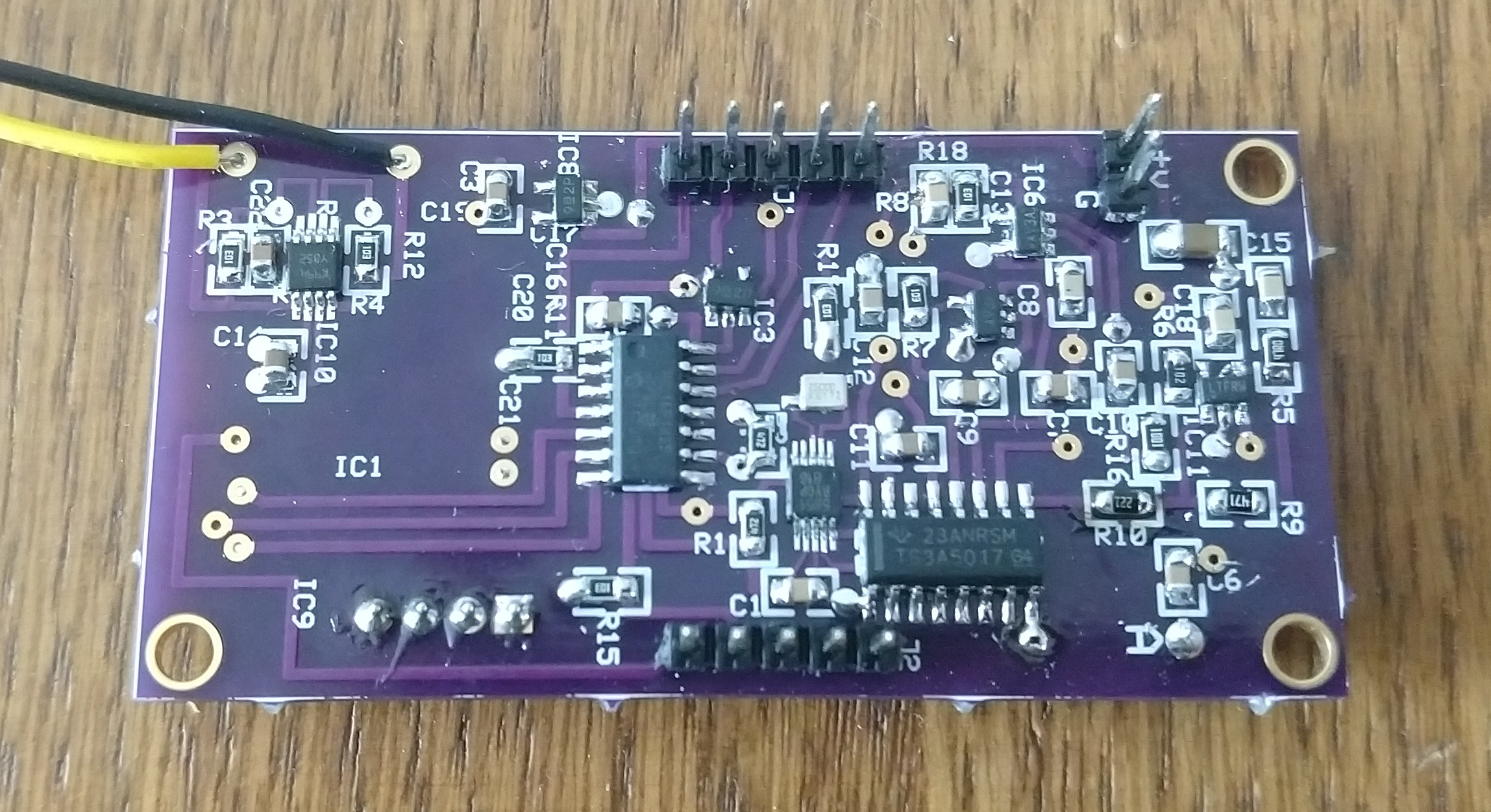
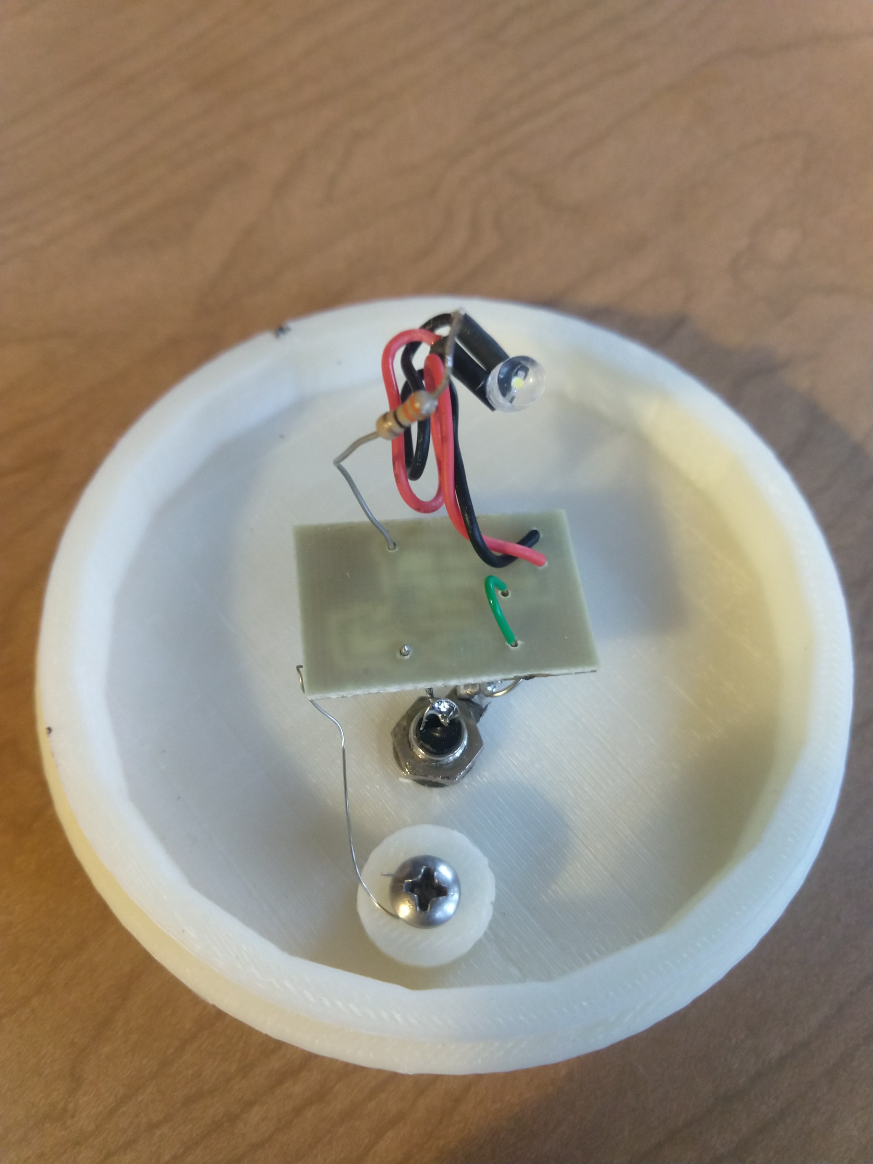
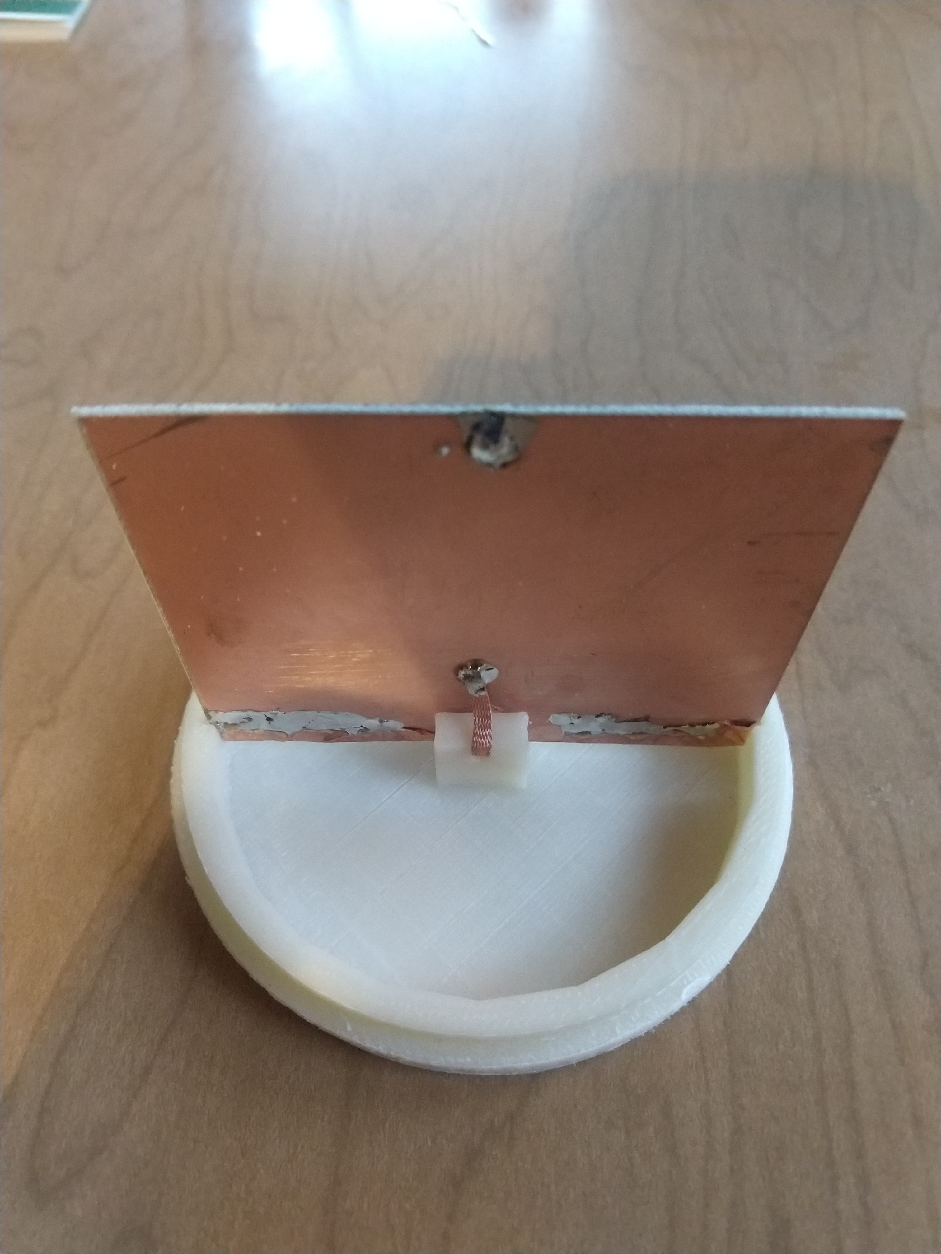
Top view of the circuit board:
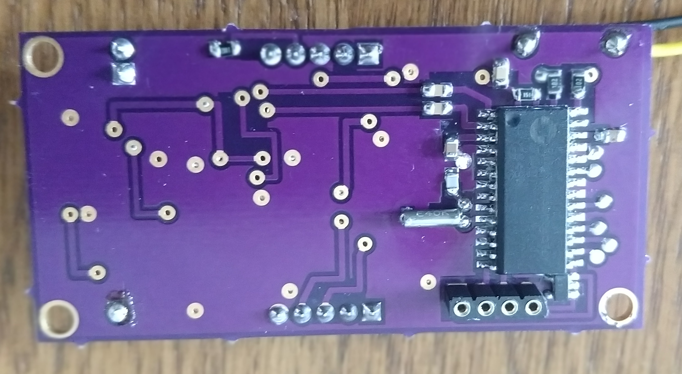
Bottom View Showing FV-1 circuitry
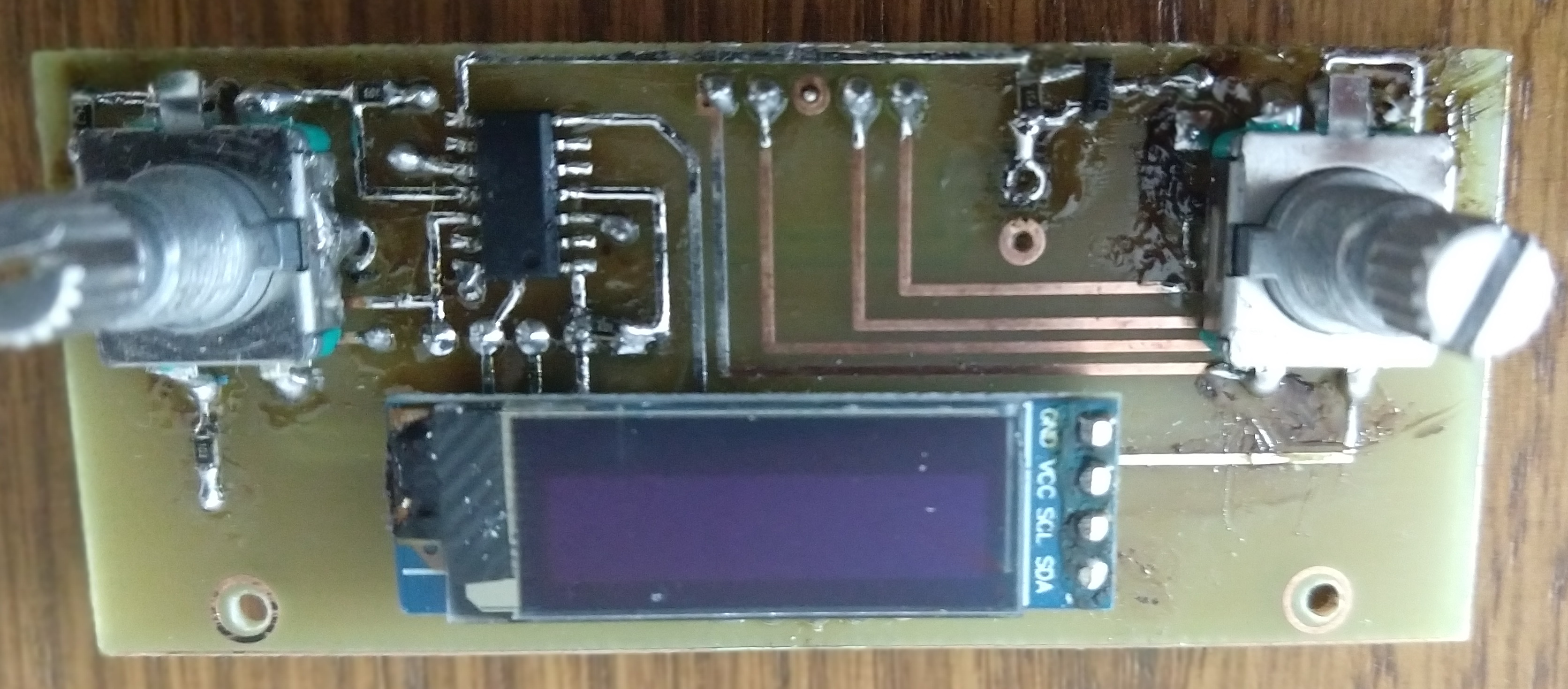
Display board
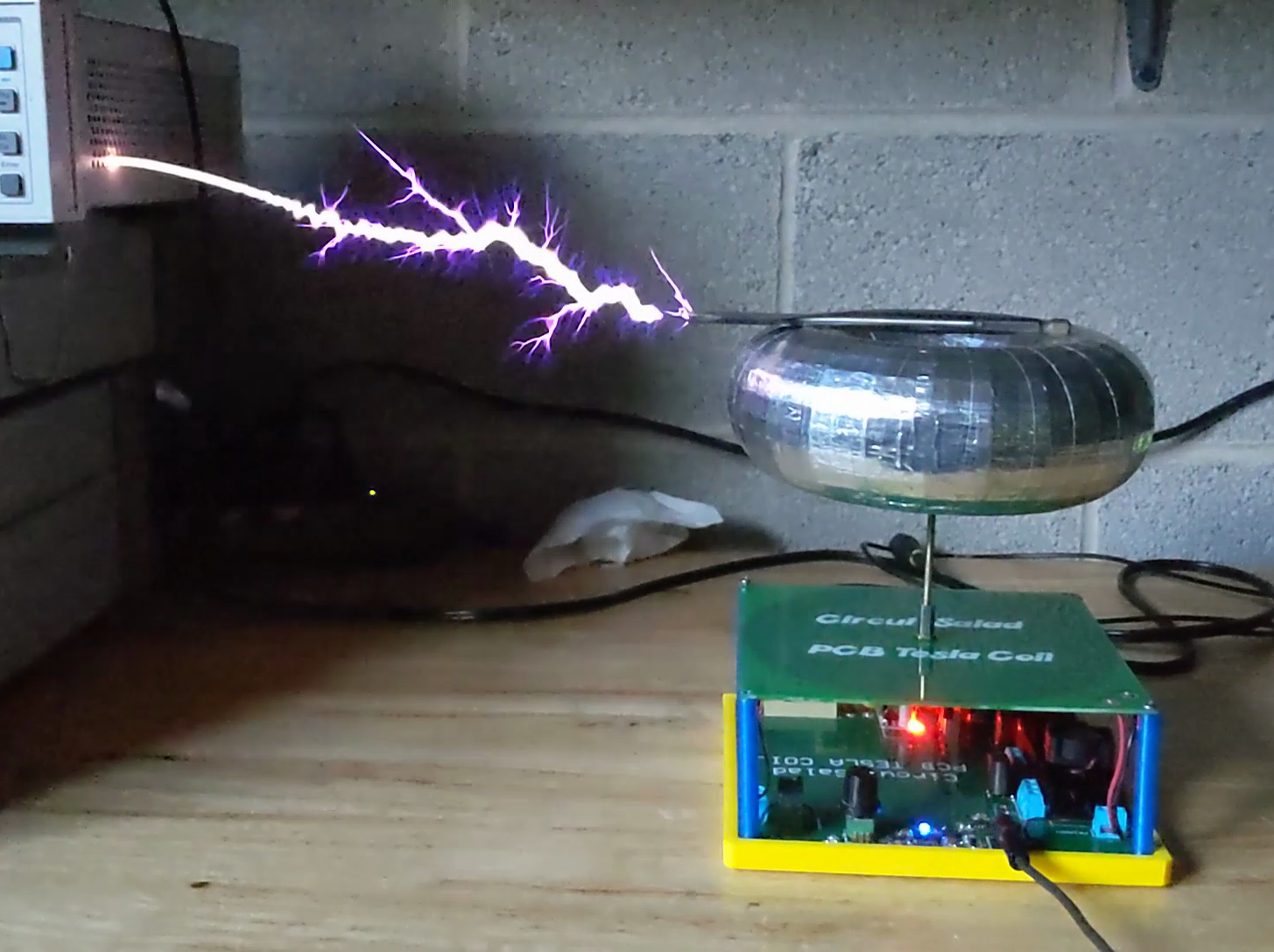
Completed Radio

Demo Videos:


