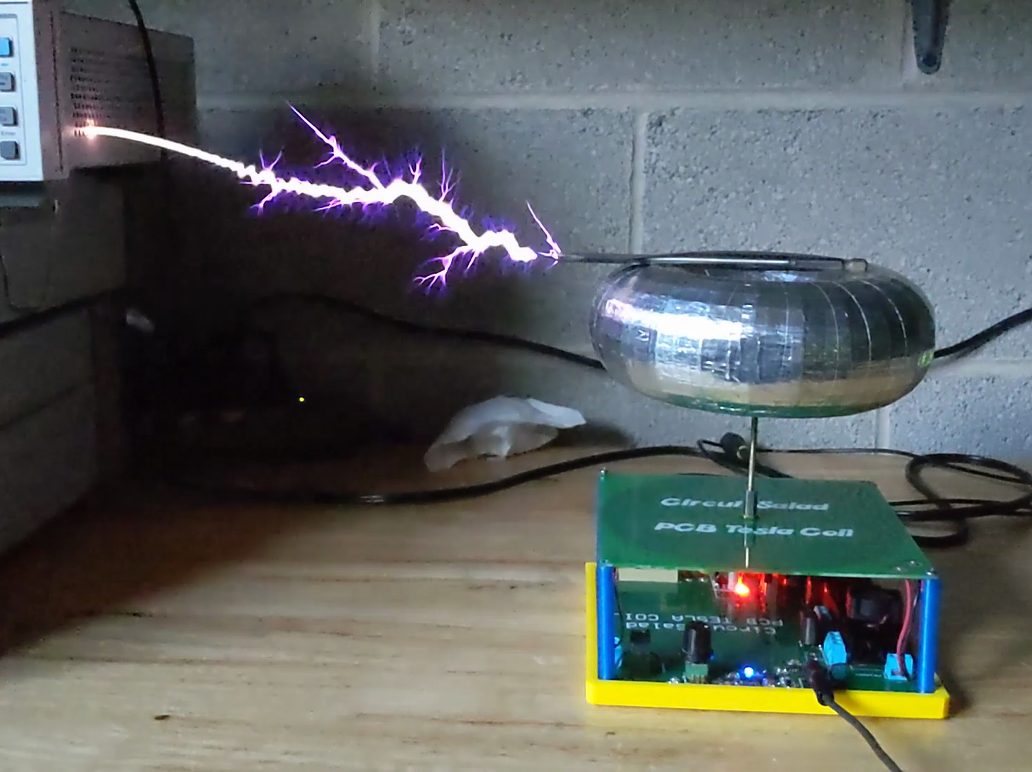
12″ Streamer from PCB etched Tesla Coil240 turn Secondary with epoxy coatingBottom Layer one turn primary
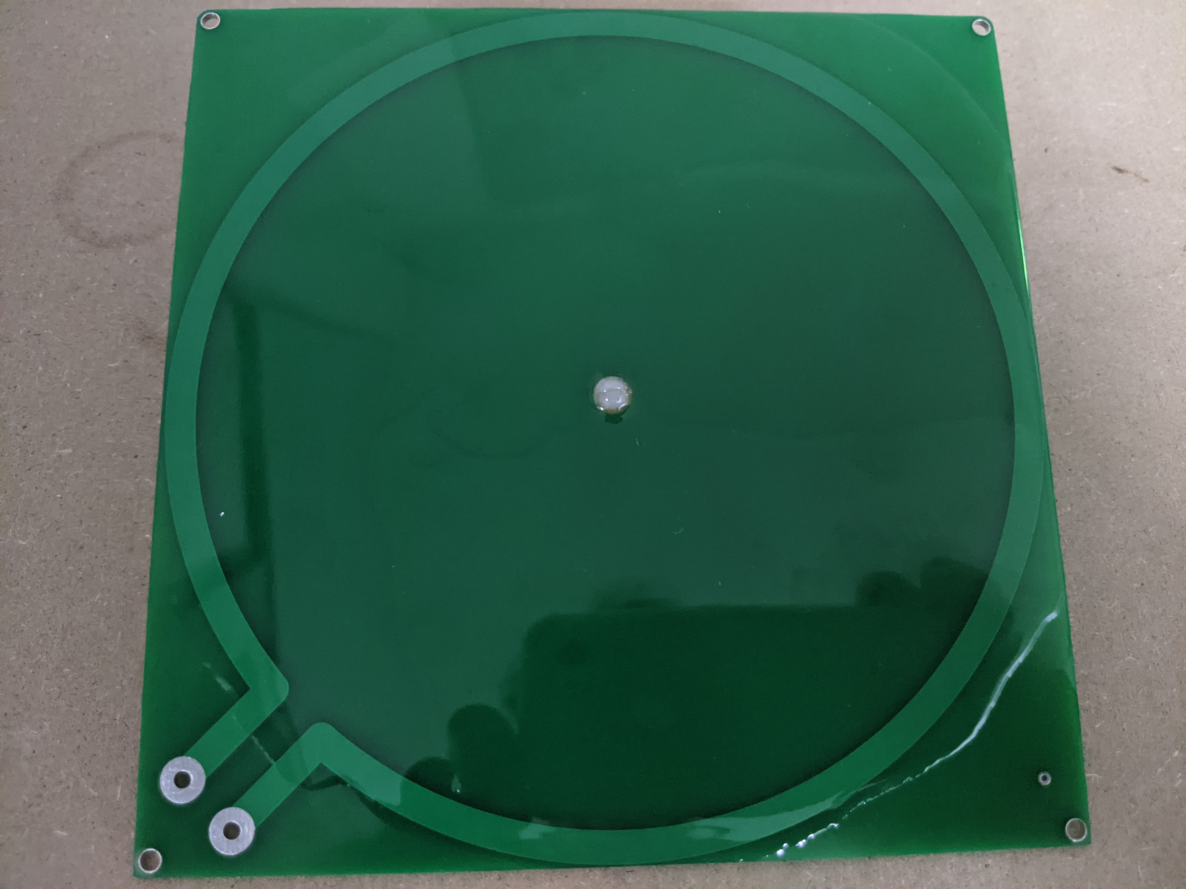
I have seen a number of low output PCB etched spiral Tesla coils on YouTube and wondered if the they could be driven to produce the larger outputs of traditional cylindrical coils. After designing my McTesla Tesla coil, I decided to try driving a PCB etched coil with my non resonant half bridge driver circuit. I first etched my own home brew coil which was 150 turns with an 8 mil trace spaced 8 mils. This worked with modest output but the frequency was higher than I desired at more than 2 MHz. So I broke down and had a commercially etched board made which was 6 inches square and has about 240 turns with a 6mil trace spaced 6 mils.
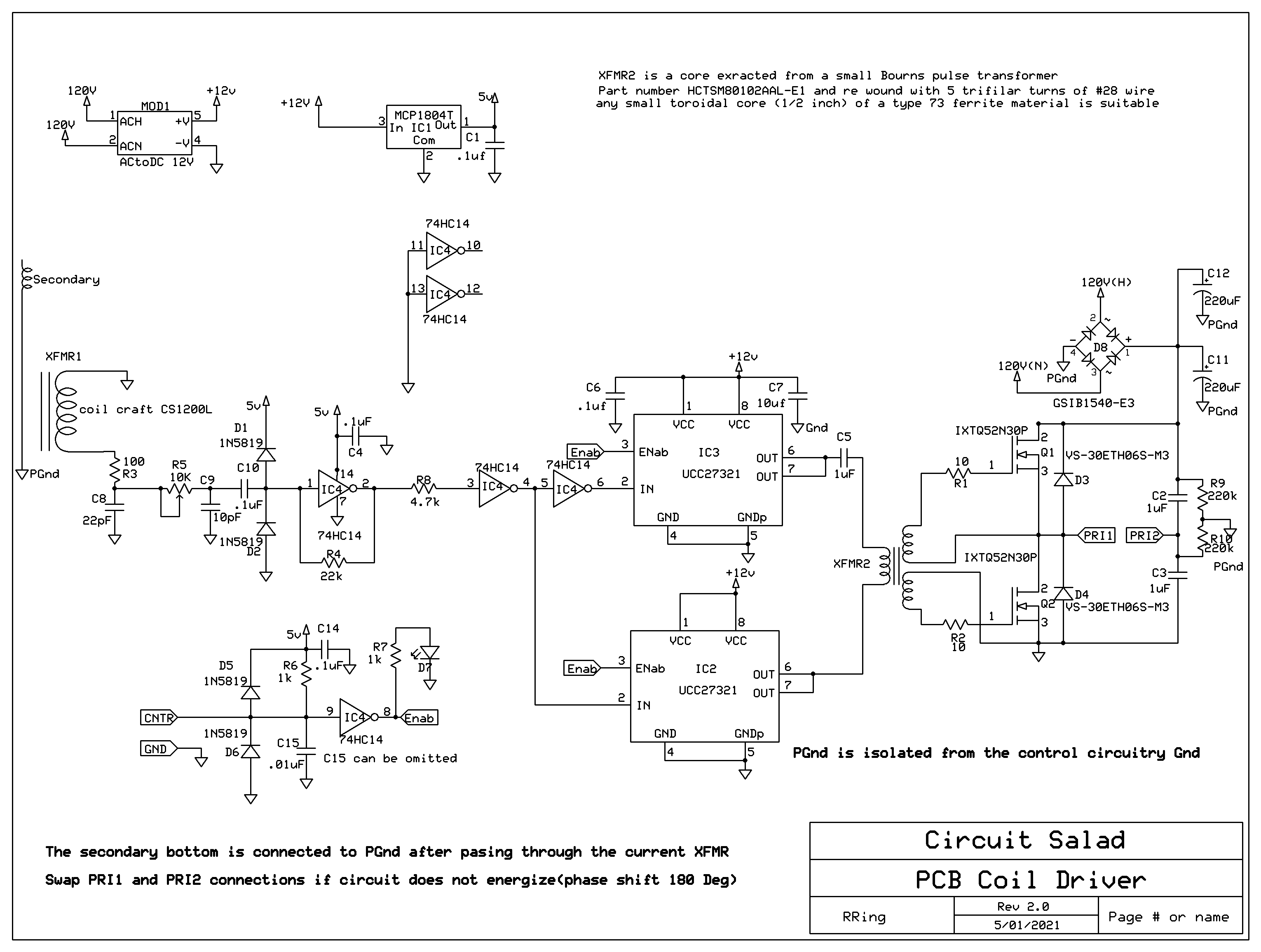
This coil performs well and depending on your top load resonates at anywhere from 900 kHz to 1.2 Mhz. The driver circuit is essentially the same as in my other designs. There are minor tweaks of the phase shifting network in the feedback path because of the higher frequency but everything else is the same. My top load is a 3D printed toroid which was wrapped in aluminum tape. The primary is one turn of etched on the bottom layer. Though the coil works quite well, it has to be carefully structured to avoid inter coil arching and breakdown.
My other coil designs utilizing this half bridge driver can achieve 9-10″ streamers. Surprisingly, the PCB etched coil can produce 12 inch streamers. To achieve such high output without the coil breaking down; I had to encapsulate the secondary in two part epoxy compound. Also the center post, connected to terminal, is screwed down to the secondary center with a nylon screw. A brass washer soldered to the center is the secondary output connection. There can be no metal screw passing through the PCB or it will fail to the primary or arc across the secondary on the top. Two part electrical potting compound works well to protect the coil and is easy to apply. It will harden in about an hour in a warm oven (170F). Both the top and bottom are potted. This coil uses the same interrupter circuit as the McTesla. The break out point is critical and the mosfets will immediately explode if the breakout point is not present. The breakout point can point up or to the side, but you have to be careful to make it extend an inch or more out from the terminal to provide adequate break out.
The McTesla is small 1000 watt half bridge Tesla coil with 3D printed forms for the terminal, secondary and the enclosure. The plastic used was PETG, which has low dielectric loss. The primary is 4 turns of 16 gauge automotive hookup wire(thick jacket) separated from the secondary about 1/8″ by means of 3D printed spacers. The power is provided directly from the mains through a half wave rectifier. The actual foot print is for a bridge rectifier but with a jumper wire you can fit the selected single diode on the board. Either will work fine. I get a little more crackle out of the half wave version so I just left it in place.
The secondary is 5″ tall and 3′ in diameter at the bottom and 5″ in diameter at the top. This alters the distribution of inductance of the coil and all but requires you have a substantial top load to suppress corona on the upper part of the winding. I get larger arcs with the conical secondary than an equivalent cylindrical secondary…maybe an inch or so more spark. I need to analyze why this is the case in more detail. The math shows a drum coil with equal diameter and height produces optimal Q. However, I think I am getting better primary coupling and impedance match allowing more energy couple to the secondary. It is wound with 700 turns of 33 gauge wire and resonates at 350 kHz. I tried 27 gauge wire and it worked fine. It resonated at 600kHz and streamer length was a couple inches less. Anything between 33-28 gauge will work well.
I have tried all sorts of different finishes for the secondary, including: polyurethane, and two part epoxy, ultimately, I ended up using 3 coats of spray shellac. It dries very quickly and you can apply 3 coats within a couple of hours. I found that when the coil is properly tuned and primary coupling is correct, a heavy insulative finish is not required.
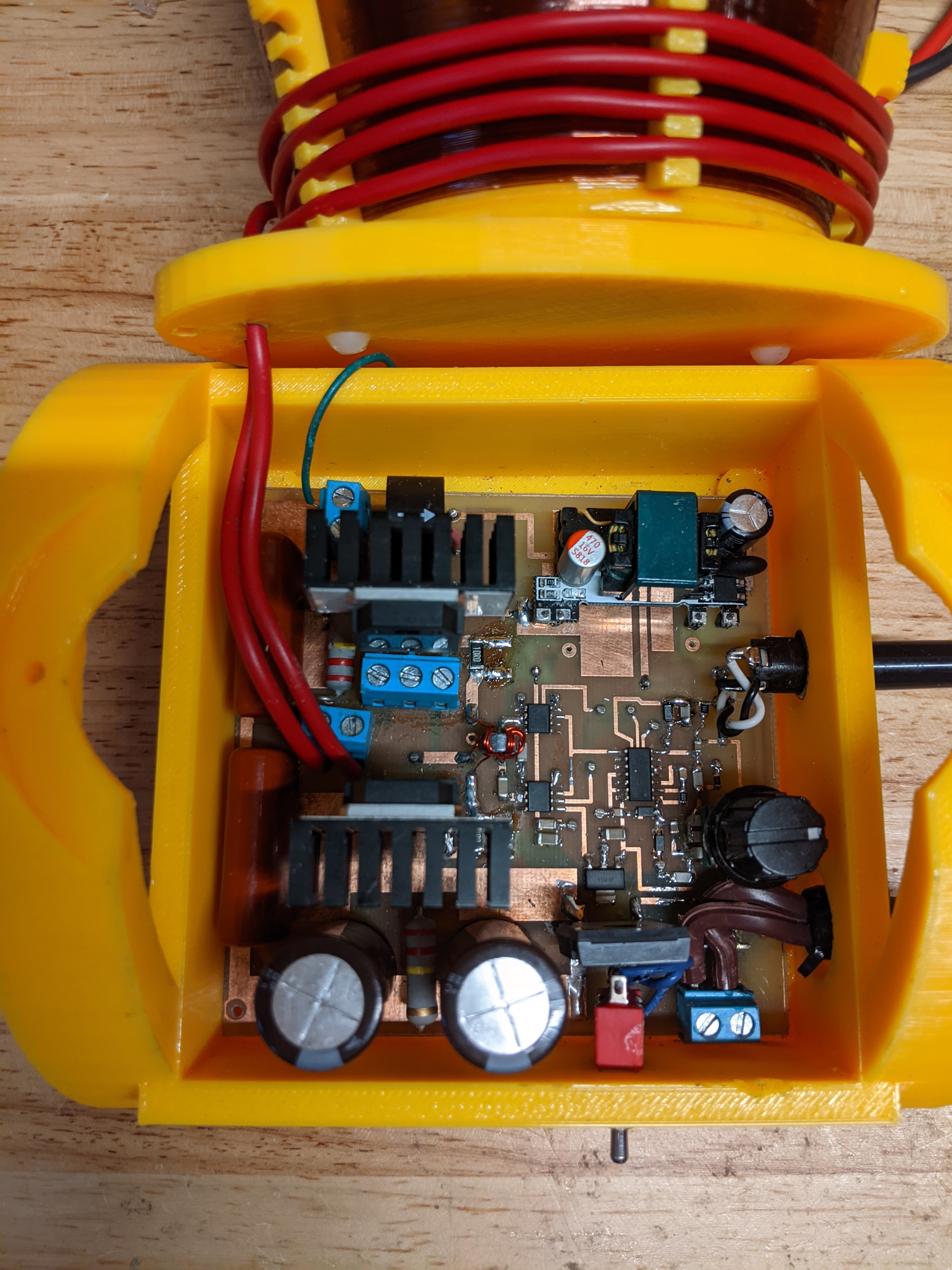
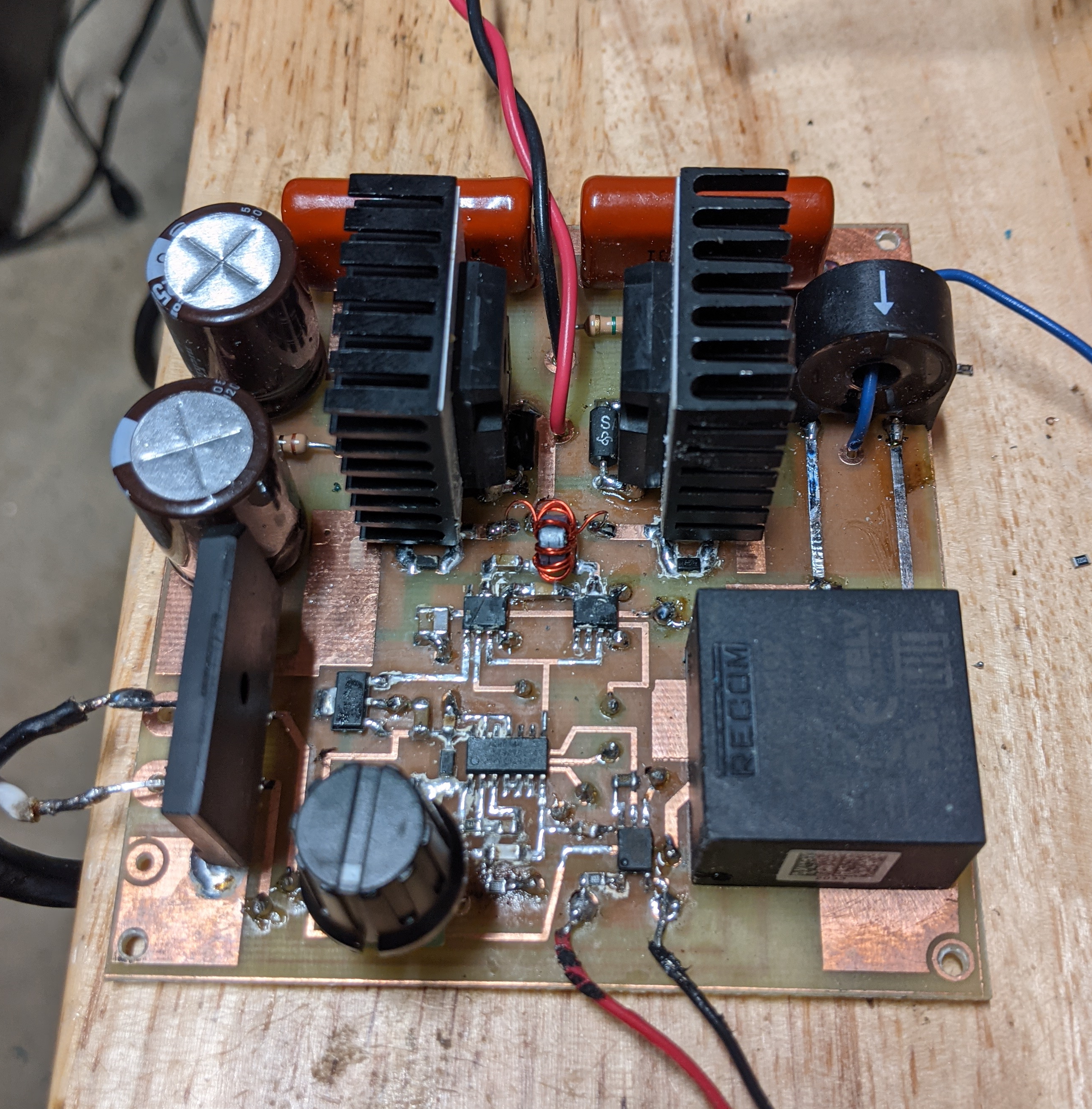
The half bridge architecture I used for this is described in more detail in a previous blog post: https://wordpress.com/post/circuitsalad.com/1875 . The main feature is the inclusion of a simple passive adjustable phase shift network in the feedback path. This allow one to minimize switching losses by minimizing current and voltage overlap in the mosfets. The end result is the FETS are less stressed and need less heat sinking. In this design, I have made some minor changes from the previous circuit. I am now using the IXTQ52N30P 300V@52 amp mosfet instead of the IRFP4229. The first IRFP4229’s I got worked great but then the next two I ordered failed quickly. As well, they seem scarce and hard to source so I thought it best to try another. The IXQ52N30P is near indestructible and I have yet to blow one. I simplified the modulation input circuit and decided to remove the diodes I was using across the gate drives. The diodes were in place to ensure the mosfets were not both conducting at the same time but I found when properly tuned, this not needed. I also used terminal blocks for the mosfet connections for easy experimental swapping or replacement . You can see this on the picture of the circuit board below. The driver board uses a 200:1 current sensing transformer for magnetic feedback to generate self excitation. This feedback signal is then phase shifted with a two stages of RC low pass filtering. One stage is fixed and the other adjustable. The adjustment range is from about 1 MHz to 200 kHz and is very forgiving. Optimal adjustment can be achieved by use of an oscilloscope, but simply tuning for the largest spark and then reducing the resistance of the POT slightly works well too.
It includes native expresspcb cad files, schematics, gerbers, 3D print files and software development files
If anyone is interested in building this device everything you need is provided in the download. I am sure there will be questions which I am happy to answer. The interrupter is not required and can be replaced with a momentary switch or any other modulated switch closure. Some of the component choices are non-critical; such as 1N5819 diodes. The UCC27322 can be used instead of the UCC27321. The gate drive transformer can be any small 73 type ferrite material balun core or toroid. Other current sensing transformers will work but the CS1200L is a good choice and available. Certain IGBT’s will work well as well as other mosfets. You may need more heat sinking depending on the device selected. The AC to DC 12V module is a cheapo pcb module from Amazon. https://www.amazon.com/dp/B07SJRX9R6?psc=1&ref=ppx_yo2_dt_b_product_details
McTesla Schematic
10″ Streamer with the McTesla
View of the McTesla circuit board
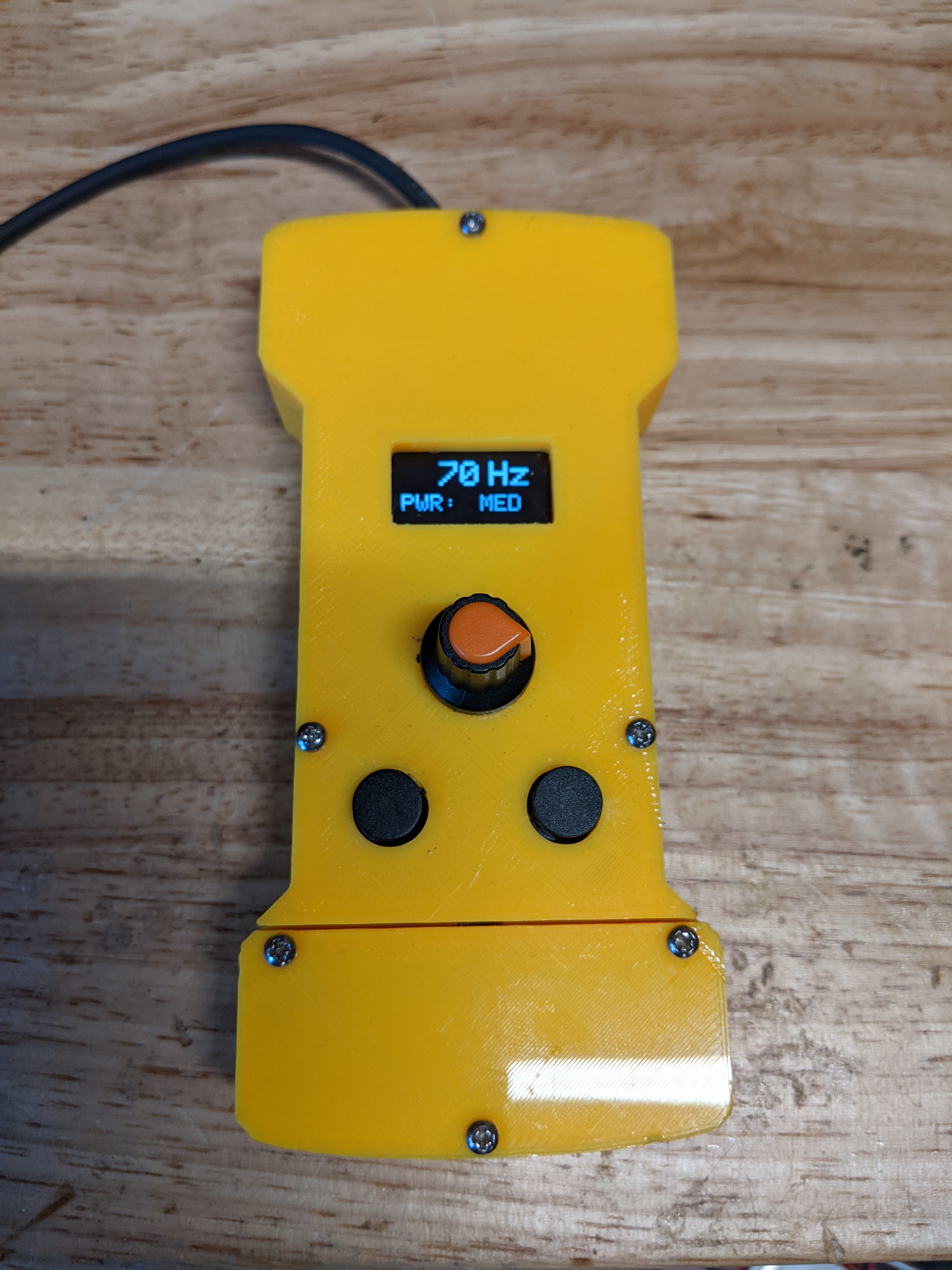
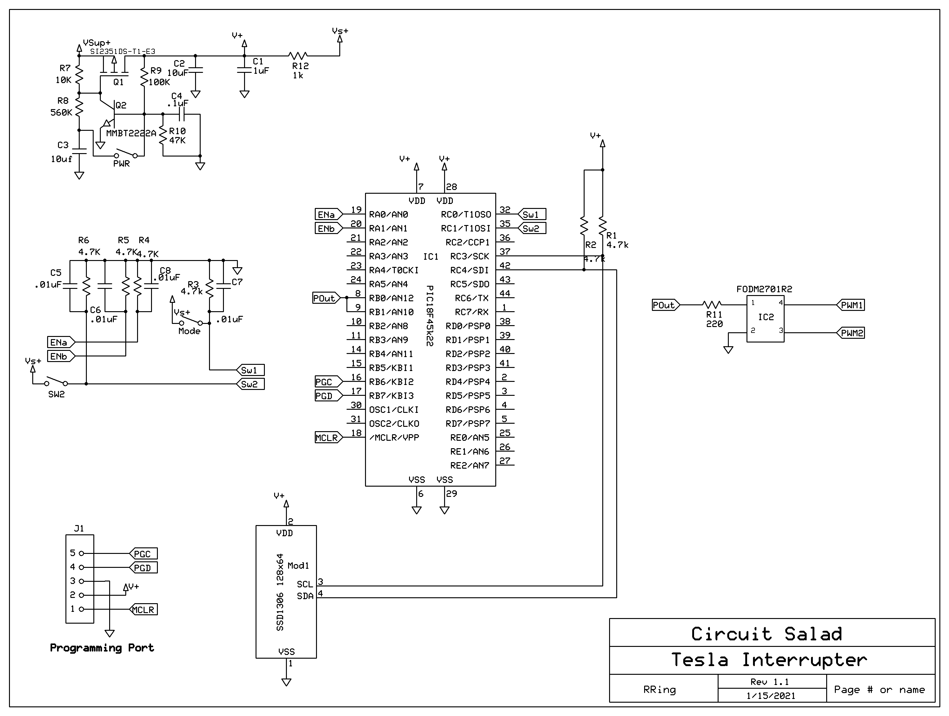
The Interrupter circuit is based on a PIC microcontroller and uses a simple opto- isolator as a transistor switching output. The OLED display used is a common 128×64 SSD1306 type. Ironically, I didn’t use the PWM output on the chip and created my own in software….but you easily could. I have it setup to provide 4 different duty cycles up to 50% , which can be adjusted by means of the two buttons. A rotary encoder sets frequency from 1hz -220Hz. I have driven the coil with 20Khz and it works. The momentary switch on the encoder is used to turn on and off the device. The software was written in C with the MikroC pro compiler. Next, I will make a PWM modulator to play music!
Lately, I have been experimenting with solid state Tesla Coil design ideas and after many destroyed mosfets, I have developed a reliable and efficient conventional solid state half bridge Tesla Coil driver. The topology is a basic half bridge so the primary is not resonant. This choice was made so I could operate it in continuous mode when desired. It is designed to operate with 120 VAC. The circuit is self exciting, utilizing current feedback from the secondary by means of a small 200:1 coilcraft current sensing transformer. The driver is efficient requiring minimal heat sinking of the mosfet switches. As such, the driver can be run for long intervals. The limitation on run time is constrained by the coils(secondary and primary ) and the electrolytic power supply capacitors heating up. I can generate 11 inch streamers on my 5″ diameter x 7″ tall secondary with a 6″ toroid terminal. I can just change out the different secondary and primary combinations I want to test, as the driver will easily operate from 100Khz to over 1 MHz. Depending on the frequency, you may need to change one resistor. The driver board is only 3.6″x 3.6″ and including simple stick on heatsinks for the mosfets.
Complete Half Bridge driver board with opto-isolator input
Demo of Driver Circuit with Small Coil
Features that improve efficiency and reduce mosfet heating:
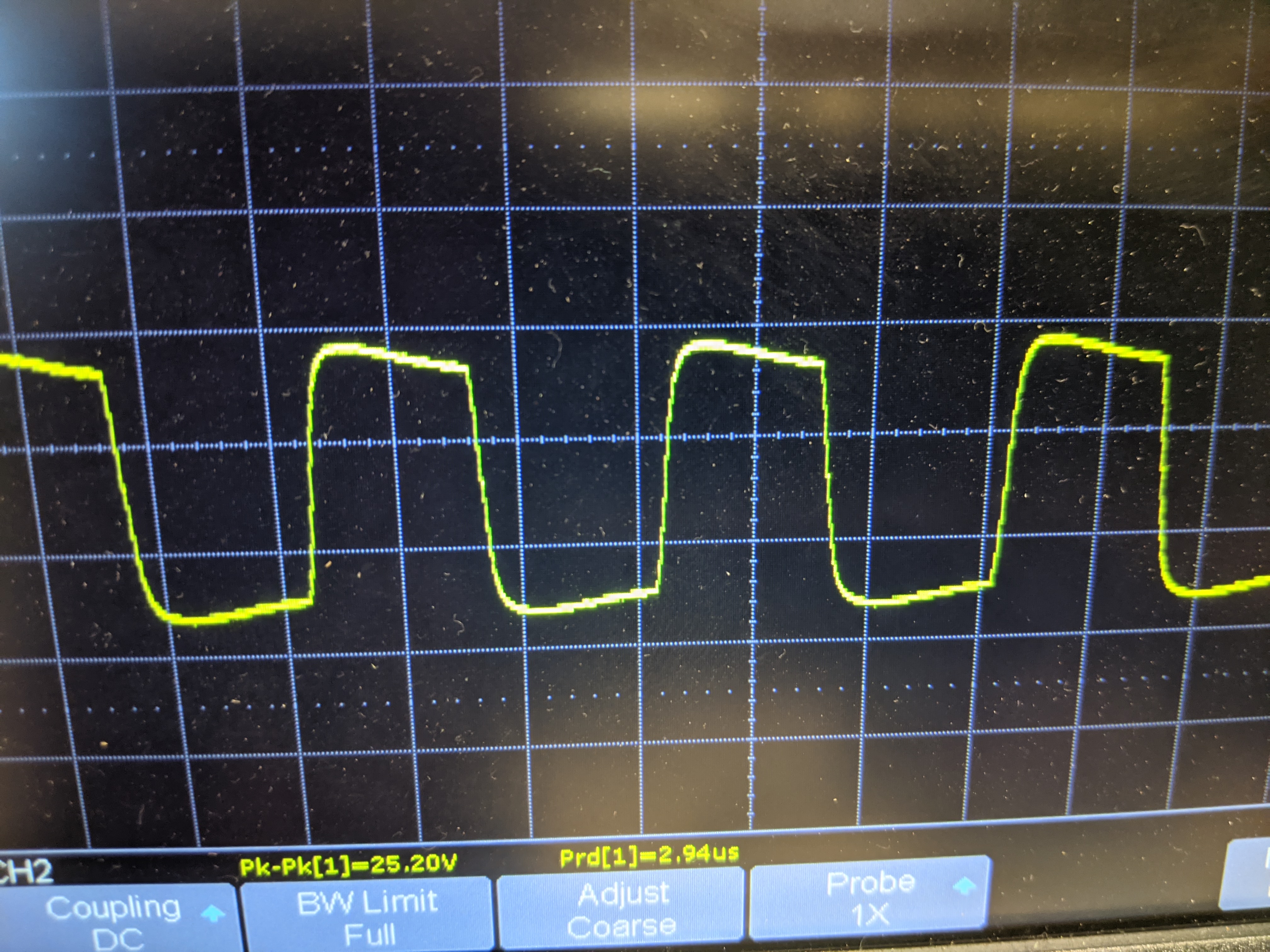
Properly designed gate drive: I used an appropriately sized and correct ferrite material xfmr core for the drive transformer. The core I used is very small (.3 inches) and was cannibalized from a small pulse xformer obtained from Mouser(photo below). There were no cheap small cores available on Mouser so i just found a small pulse isolation transformer that was inexpensive and I could get the core from. If you prefer, you can purchase stand alone core. Type 73 material is a good choice and a core no bigger than a .5 inch will be fine for this circuit. I cannibalized the core out of the housing and re-wound it with a trifilar 28 gauge winding of 5 turns. I also placed schottky diodes across the 10 ohm gate resistor providing for slightly faster off time than on time, This ensures minimal shoot through(both mosfets on at the same time). The drive is clean with no ringing and fast rise and fall times(pictures below). This reduces switching losses.
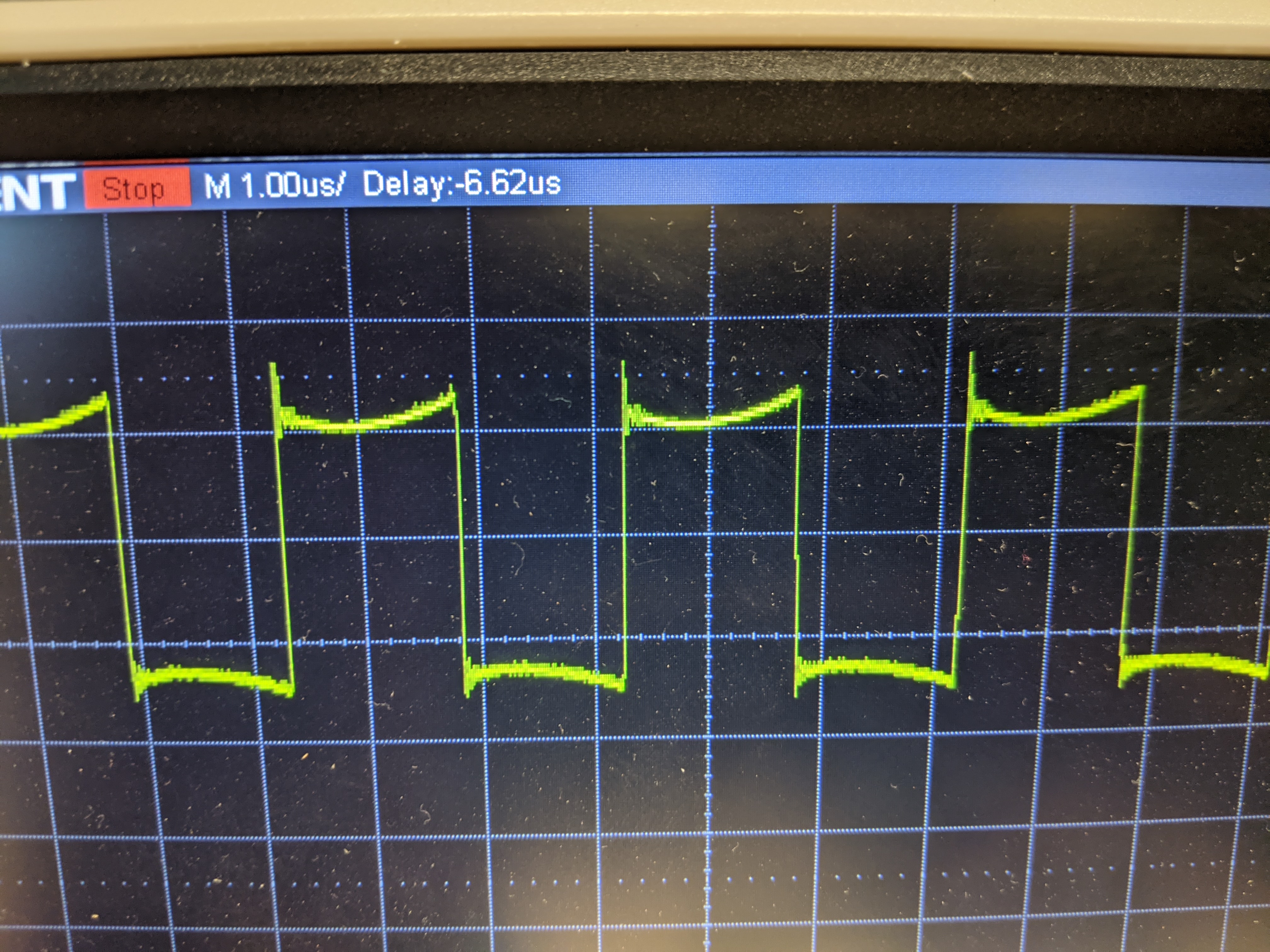
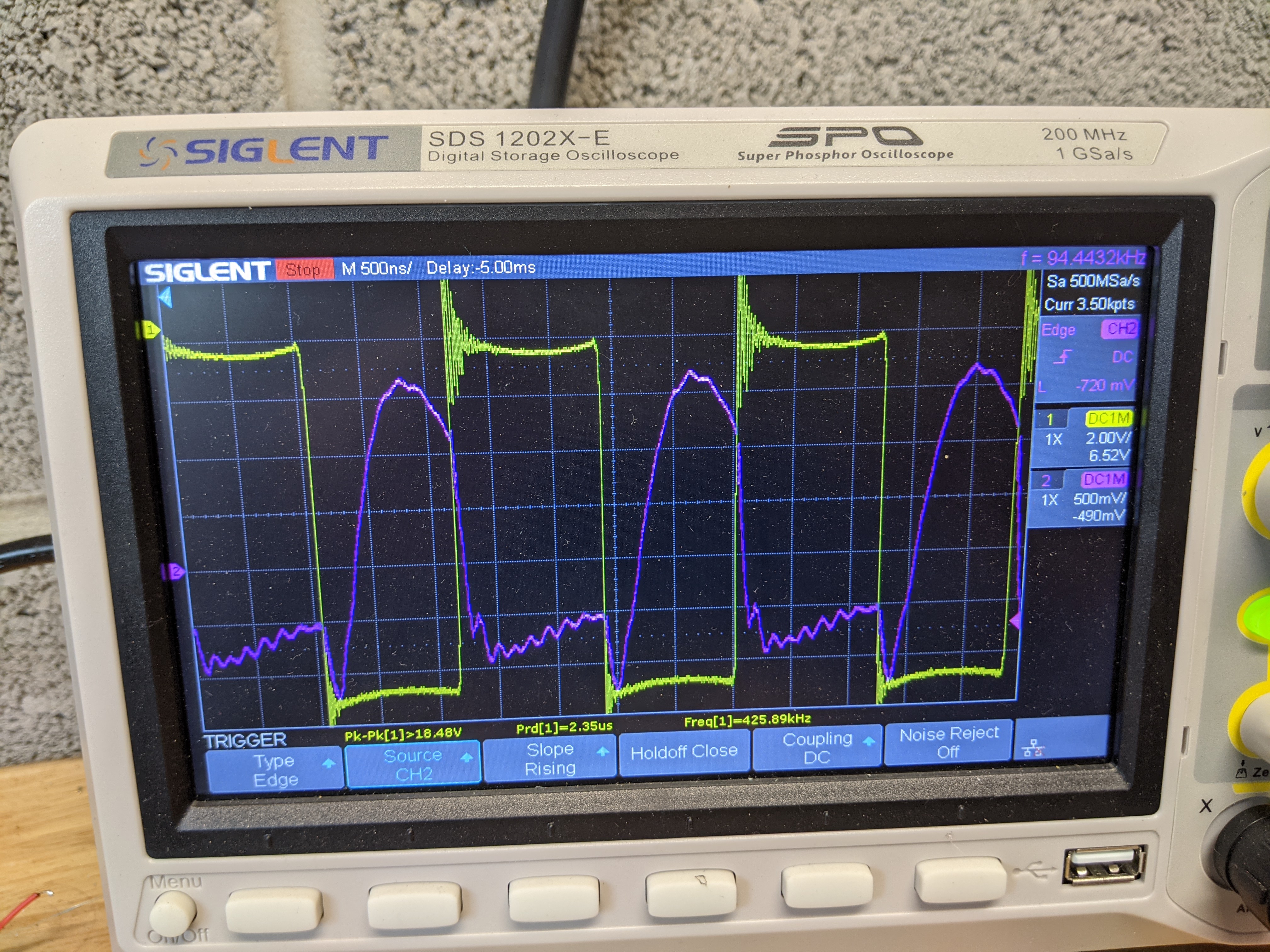
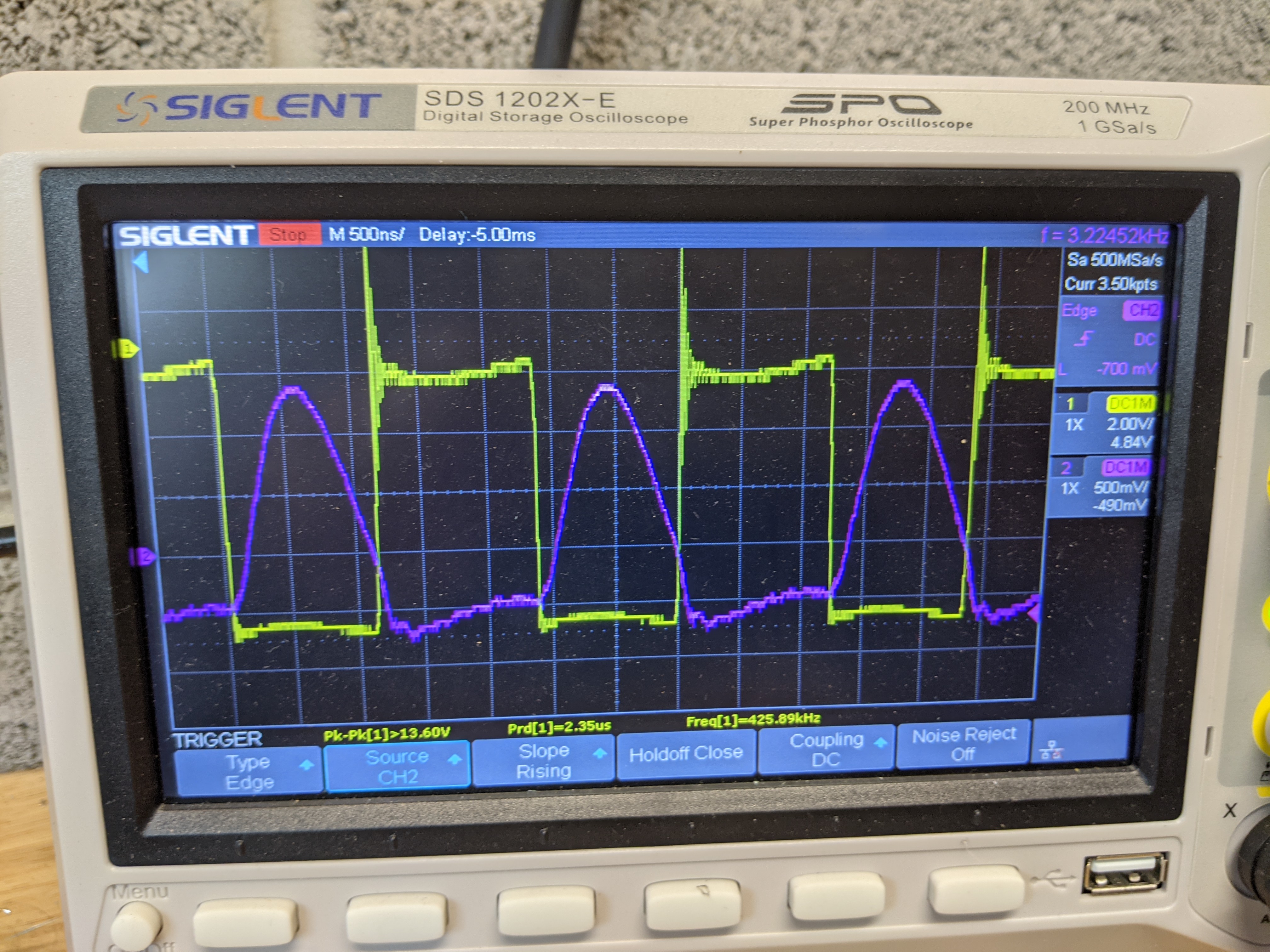
Drive signal as seen from mosfet gates(no ringing)Output switch waveform as seen from drain of mosfets(very little ringing)
Choice of mosfet: I wanted to select a low cost and high performance mosfet for the circuit. There are two I found that work well. The basic criteria are : > 250V breakdown rating @ > 20 amp current capacity. Low output capacitance, gate capacitance and on resistance were also important. The IRFP4229 is the ideal candidate. It has a breakdown of 250V. It can handle 40 amps of current, and has total switch delay of of 100ns(very fast). The on resistance is .04 ohm; so IR losses are low. A similar device, only slightly slower and with a slightly greater on resistance is the STW46NF30. Both were evaluated and worked well. The cost of both of these mosfets is around $3 each.
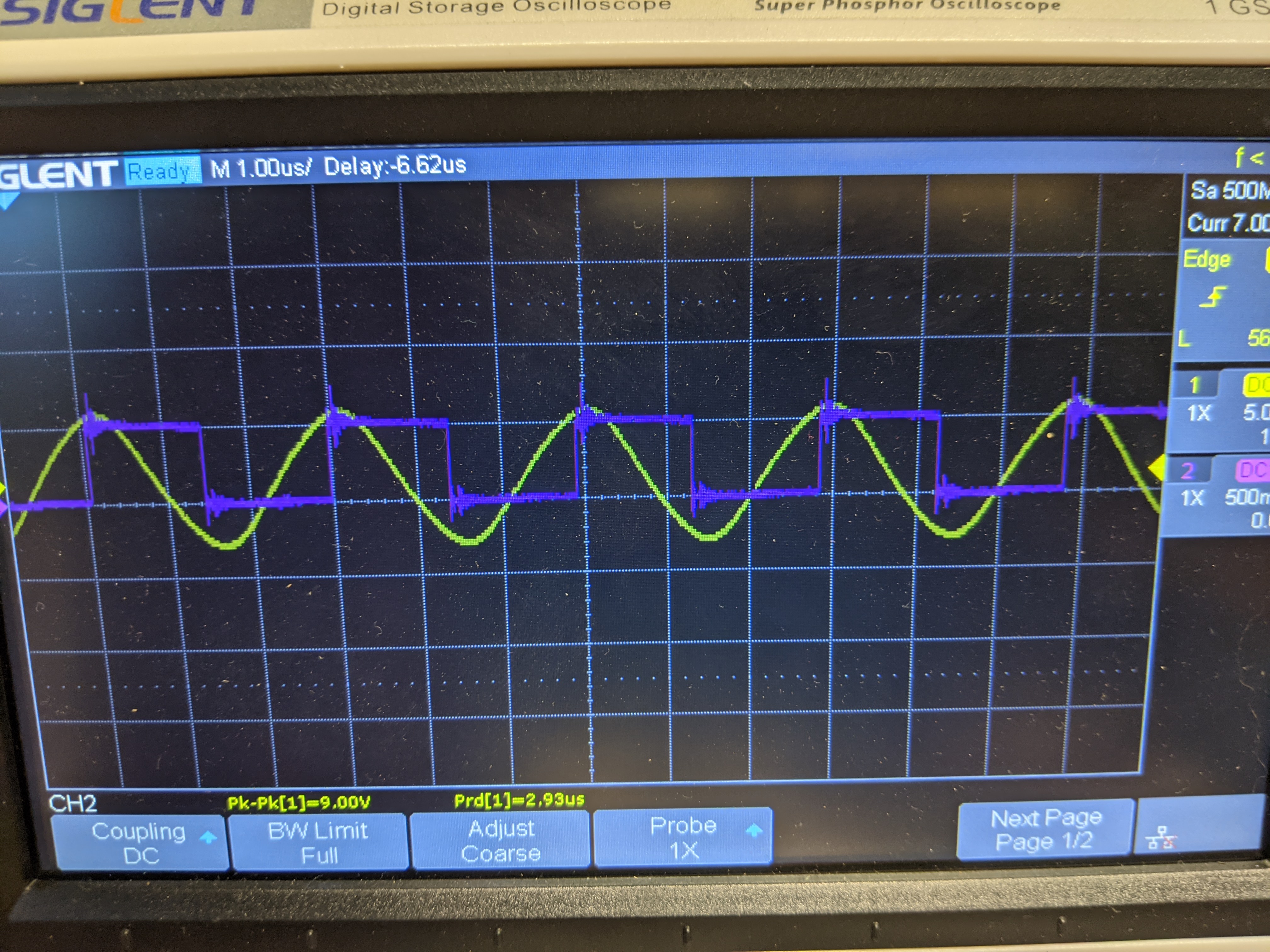
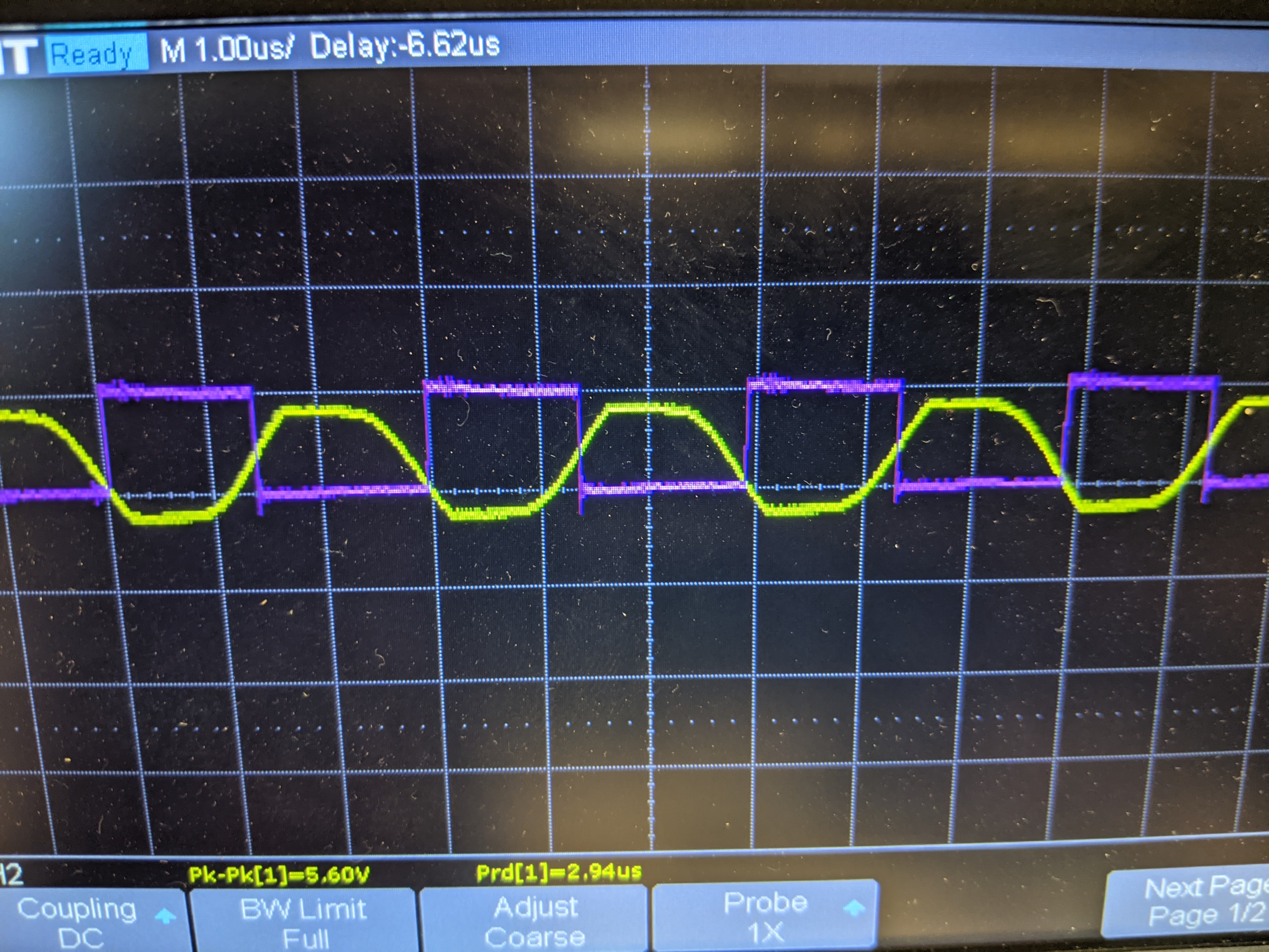
Adjustable phase shift control in feedback loop: A substantial improvement in output and efficiency was obtained by placing a simple low pass RC phase shift network in series with the secondary feedback path. It was observed that when my test coil was driven from an external source, the input drive was approximately 90 deg out of phase with the secondary output. This was the case when the coil was tuned for maximum output. This amount of phase shift will not support oscillation properly. Forcing the coil to self excite will not produce optimal output unless some sort of phase shifting is employed. The notion that a self excited tesla coil will inherently tune itself to best performance is incorrect. Adjusting the input /output the phase relationship maximizes coil output but also lets one adjust the drain voltage/current relationship such that zero crossing switching can be obtained. This is when the current and voltage across the switches do not overlap. This greatly reduces power losses across the switch. The phase shift network consists of two simple RC low pass filters in series. One with a fixed resistor and the other is a variable resistor to allow adjustment. The low Q nature of the RC filter provides optimal tuning over a wide range and is easy to adjust and is stable. The values for the filter as shown in the schematic are easy to calculate. Simply pick a resistor value(10k for example), then use the approximate value of operating frequency(+-20% is fine) to determine the capacitors required. The value of capacitance is correct when the reactance of the capacitor at the given frequency is the same as the resistor value(10k). Or chose a capacitor value such as 47pf. With this value, the reactance at 650KHz is 1/2Pi(650KHz)(47pF), which is 5212 ohms. So you could use a 4.7k resistor for one RC stage and a 10k to 50k pot for the second stage. In my example coil, the frequency is around 400KHz and so I used 10k with 47pF and a 25K Pot with a 47 pF for the second stage. The low pass characteristic of the phase shifting also has the benefit of reducing higher frequency noise and parasitics in the feedback loop. The result of this simple addition to the circuit is substantial and when you tune the variable resistor you can see the output significantly increase and decrease. You can monitor the drain voltage and current to adjust phase for optimal performance. Alternatively, I have found that you can simply adjust for longest streamer length and then add just a tiny bit more phase shift to optimize switching efficiency.
Input to output relationship before phase shift addedInput to output phase relationship after phase adjustmentDrain voltage and current(purple) when poorly tunedDrain Voltage and Current when phase adjusted for maximum output and lowest switch loss
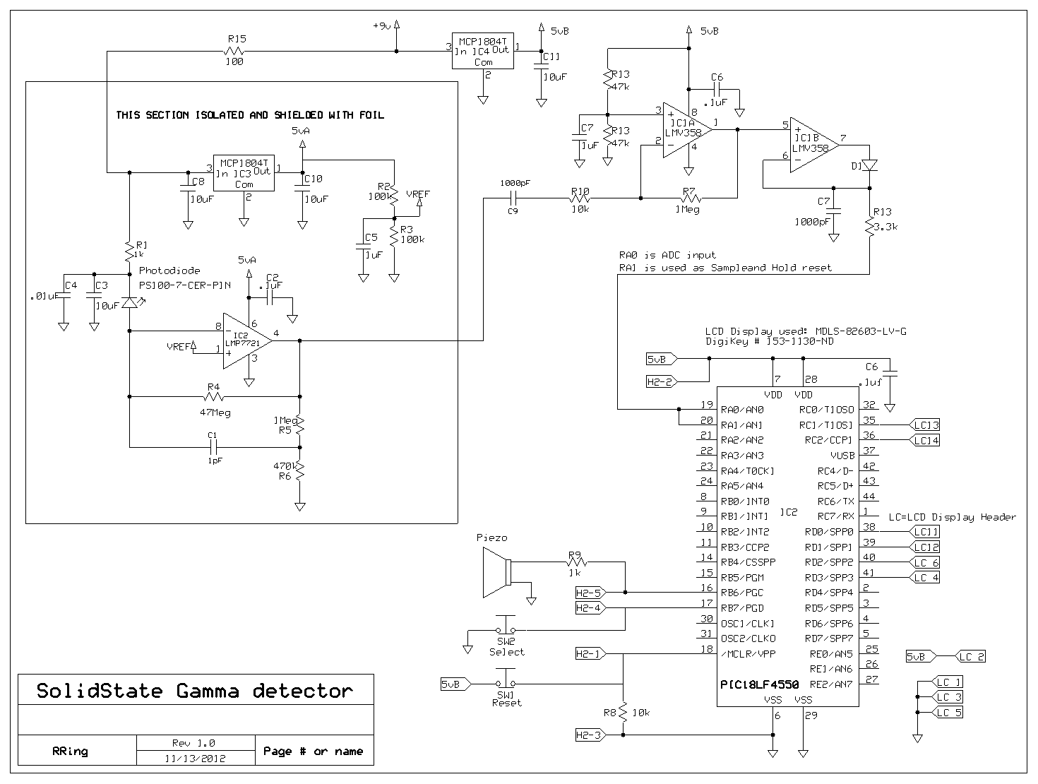
I added a PIC and LCD to my basic radiation detector and can now display total counts over time(up to 24 hours) or Counts/Sec and relative gamma strike energy level. The energy level varies as every gamma strike does not dislodge the maximum possible number of charge carriers. I take the maximum value registered every second and display. On average various materials indicate different levels, providing a crude detection signature. Besides the LCD display, this circuit has a sample and hold circuit which is connected to the PIC ADC module and also tied a another PIC I/O pin which switches from tristate to pulled low to reset the sample/hold circuit. The maximum sample rate is 13500 samples/per sec.
Photodiodes convert light into current and this current can be coverted into voltage and amplified. Sounds simple right? Well, when trying to detect Gamma photons, the design of a photodiode detector is not so simple. This circuit is not paticularly complicated, but the design took some effort and many of the component values are critical.
This circuit behaves like a classic Geiger counter, but unlike a traditional Geiger Counter you can actually measure the output pulses over time to roughly determine average energy of the gamma photons. With the addition of a microcontroller, an A/D converter and LCD – you can display all kinds of interesting data. Later, I plan to add this to my design. If you build this detector – you will need a source of radiation for testing. A cheap smoke detector can provide this (Americium-241) or import gas lantern mantles which have thorium in them. Check out ebay.
When designing such a detector, the first issue to resolve is the selection of the photodiode. The important features are: the diode area, leakage current(dark current), and capacitance.You want the capacitance to be low as possible, the diode area large as possible and the reverse bias leakage current as small as possible. Unfortunately, the larger the diode area, the worse the leakage and capacitance become. A large diode is desirable to provide more area for photons to strike. Gamma photons create a transient current charge on the photodiode, so if the capacitance is to large, the photon strike transient is absorbed and not detected. By reverse biasing the photodiode, the depletion region is increased and the capacitance is significantly reduced. The reverse biased mode of operation is called photo-conductive mode. However, the reverse bias creates leakage current which generates noise. The gamma photons produce very small charges and the output is very close to the noise floor; so care must be taken to minimise all noise. Having said this, reducing capacitance appears to be more beneficial than the noise of the dark current is detrimental. This is because you need the frequency response to capture the transient of a gamma photon event. Using the highest bias possible is generally preferable. Not only do the gamma strikes produce higher output, but the stability of the amplifier circuit is improved allowing for more charge gain.
The photodiode I am using is very large. It is 10mm x 10mm and has 80 pF of capacitance under bias and about 2-4 nA of leakage current. It is the PS100-7-CER-PIN the performance is excellent but it is very expensive. A much lower cost alternative photodiode is the BPW34. However, it is less than 1/10 the area and will require closer proximity to obtain photon strikes. On the bright side, its capacitance is much lower.
The first stage of amplification for the photodiode is a transimpedance amplifier. Which is a current to voltage amplifier. The impedance of the photodiode is incredibly high requiring an OP amp with input bias currents of picoamps or less (minimizes loading of the photodiode) and bandwidth greater than 1Mhz as the photon strikes generate pulses from 100KHZ to 50Khz or so. The noise figure of the op amp needs to be very low. Also the OP amp should have low input capacitance so as not to create further high frequency loss. The OP amp I chose was the LMP7721 which has a bandwidth of 17 mHz, an input bias current of 3 femtoamps(amazing) and an input capacitance of about 8pF. Other amplifiers will work. Another good choice is the LM6211 which has even less input capacitance and picoamp bias current. Both of these amps have very good current and voltage noise figure specs.
The feedback resistor R4 is gigantic at 47 Meg and with all of this gain in tandem with the input capacitance of the photodiode, the whole thing will become an oscillator so a compensation capacitor is required across the feedback resistor. This capacitor value can be calculated by means of the formula:
Ccomp = 1+sqrt(1+4Pi*Rf*Cin*unity gain bandwidth)/(2Pi*Rf*unity gain bandwidth).
Ignoring the two “+1’s” :
Ccomp = sqrt(4Pi*47M*80Pf*17MHz)/(2Pi*47M*17MHz)
In my case, the Cin is 80pF, unity gain freg is 17Mhz and Rf 47Meg. When you do the calculation you will end up with .2 pF which is so tiny, it is not practical. To solve this, I use the resistor network formed by R5 and R6 to allow for the use of larger value capacitors. As long as the resistors R5 and R6 are much smaller than Rf, the effective capacitor value is reduced by the resistor ratio. The value of the compensation capacitor is critical. If it is to large gain is reduced and of course if it is to small, the amplifier will be unstable.
The second amplifier stage is the first stage of a LM358. It has a low frequency roll off at about 20 Khz to eliminate 60Hz hum and other low frequency noise. This is acomplished by the first order filter formed by C9 and R13. The second stage of the LM358 is a comparator with capacitor C12 added to beef up the pulses for better flashes and or clicks from a small speaker or piezo transducer.
As shown in the schematic, the photodiode and first stage of amplification, need to be shielded with foil to eliminate light and electrical noise. Because of this, it can only detect gamma rays or cosmic radiation , which is super charged alpha particles.
For fun, lets discuss another way to think of this detector:
In this case Cf is .5pF (.22pF + stray) and Rf is R4(49meg). The R feedback value is large so that it does not load down the photodiode but still provides feedback such that voltage at the input node stays at zero and the charge is forced onto the capacitor Cf by the feedback amplifier. It is not large to set gain in the traditional sense. If you look at this circuit as just a simple inverting amplifier, my point is easier to understand. For voltage gain, the (feedback resistor/ source impedance) would be the voltage gain of this inverting OP Amp topology. Here, the photodiode source impedance can be 100 megaohms up to gigaohms. So a feedRf of 10 meg or 47 meg doesn’t make much difference. The transformation of charge to voltage is often refered to as sensitivity rather than gain. The units would be mV/MeV (millivolts per mega electronvolts). This is a unsual amplifier in that we are trying to convert a discrete number of collected electrons into a voltage pulse.
A different way to think of this circuit is as a charge amplifier, where a gamma photon strike creates pool of electrons on the photodiode. From this, we can derive Gamma sensitivity. To do this, we need to know the energy of a gamma photon, the energy required for silicon to break an electron/hole pair (temp sensitive and approximately 3.62 eV at room temp), our feedback capacitance in the amplifier(about .5pF) and the elementary charge of an electron(1.6×10^-19).
To start with: Voltage = Q/C where Q = number of electrons (charge) and C is the Cf in our circuit.
Vout(amplifier) = Qin/Cf(which is effectively integrating all of the charge to voltage at the output).
For example: Americium-241 generates a 59Kev gamma pulse, therefore 59Kev/3.62eV = number of electrons = 16.3K electrons per gamma strike. This assumes all of the possible electrons and holes are formed , which is an ideal assumption and not realized.
Now to find Q in coulombs, we take 16.3k * 1.6×10^-19 = 2.61 ^-15 coulombs
Output Voltage = Q/Cf(C1) = 2.61 ^-15/.5 pF = 5mV
In my circuit, I amplify this output 100 X so I would expect to see an output of .5v . This is an ideal result and does not take into account stray capacitance, limited amplifier open loop gain, filter losses, and imperfect conversion of electrons in the diode, etc.
When I am lucky I see about 200 mV output from an Americium-241 source. On average, an Americium-241 source will generate a 150mV pulse. When this circuit is working correctly, there will be about 50mV to 60mV of noise. The practical detection threshold is about 100 mV.


