A Solid State Photodiode Gamma Radiation Detector

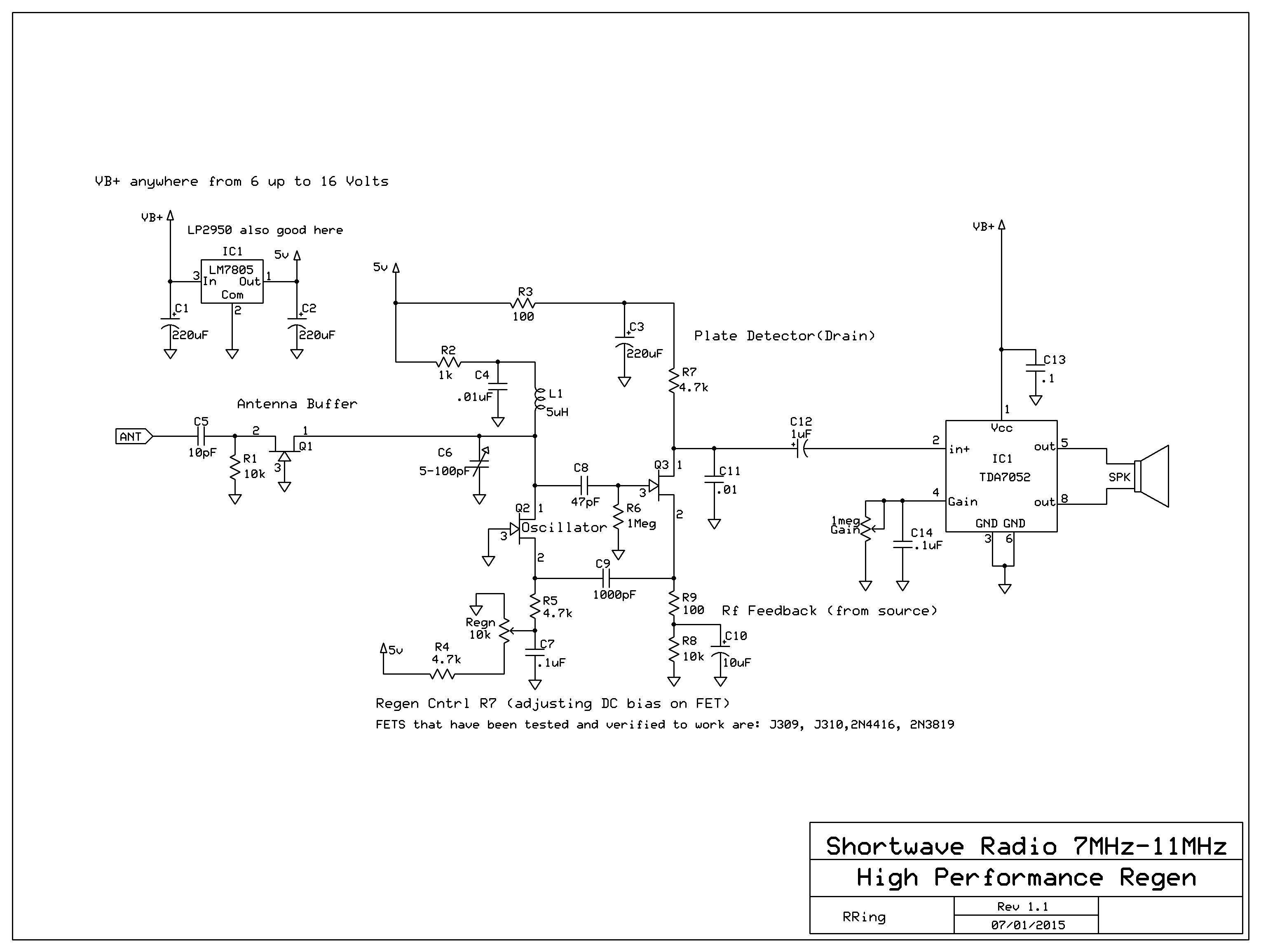
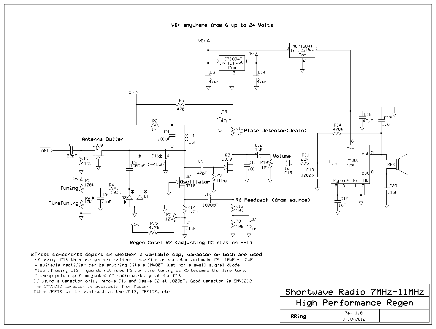
Photodiodes convert light into current and this current can be coverted into voltage and amplified. Sounds simple right? Well, when trying to detect Gamma photons, the design of a photodiode detector is not so simple. This circuit  is not paticularly complicated, but the design took some effort and many of the component values are critical.

Image of unshielded detector

Schematic:

https://circuitsalad.com/wp-content/uploads/2012/11/geiger.gif

Video Demo:

This circuit behaves like a classic Geiger counter, but unlike a traditional Geiger Counter you can actually measure the output pulses over time to roughly determine average energy of the gamma photons.  With the addition of a microcontroller, an A/D converter  and LCD – you can display all kinds of interesting data. Later, I plan to add this to my design. If you build this detector – you will need a source of radiation for testing. A cheap smoke detector can provide this (Americium-241) or  import gas lantern mantles which have thorium in them. Check out ebay.

When designing such a detector, the first issue to resolve is the selection of the photodiode. The  important features are: the diode area, leakage current(dark current), and capacitance.You want the capacitance to be low as possible, the diode area large as possible and the reverse bias leakage current as small as possible.  Unfortunately, the larger the diode area, the worse the leakage and capacitance become. A large diode is desirable to provide more area for photons to strike. Gamma photons create a transient current charge on the photodiode, so if the capacitance is to large, the photon strike transient  is absorbed and not detected. By reverse biasing the photodiode, the depletion region is increased and the capacitance is significantly reduced. The reverse biased mode of operation is called photo-conductive mode. However, the reverse bias creates leakage current which generates noise. The gamma photons produce very small charges and the output is very close to the noise floor; so care must be taken to minimise all noise.  Having said this, reducing capacitance appears to be more beneficial than the noise of the dark current is detrimental. This is because you need the frequency response to capture the transient of a gamma photon event. Using the highest bias possible is generally preferable. Not only do the gamma strikes produce higher output, but the stability of the amplifier circuit is improved allowing for more charge gain.

The photodiode I am using is very large. It is 10mm x 10mm and has 80 pF of capacitance under bias and about 2-4 nA  of leakage current. It is the PS100-7-CER-PIN  the performance is excellent but it is very expensive. A much lower cost alternative photodiode is the BPW34.  However, it is less than 1/10 the  area and will require closer proximity to obtain photon strikes. On the bright side, its capacitance is much lower.

The first stage of  amplification for the  photodiode is a transimpedance amplifier. Which is a current to voltage amplifier. The impedance of the photodiode is incredibly high requiring an OP amp with input bias currents of picoamps or less (minimizes loading of the photodiode) and bandwidth greater than 1Mhz as the photon strikes generate pulses from 100KHZ to 50Khz or so. The noise figure of the op amp needs to be very low. Also the OP amp should have low input capacitance so as not to create further high frequency loss. The OP amp I chose was the LMP7721 which has a bandwidth of 17 mHz, an input bias current of 3 femtoamps(amazing) and an input capacitance of about 8pF. Other amplifiers will work. Another good choice is the LM6211 which has even less input capacitance and picoamp bias current. Both of these amps have very good current and voltage noise figure specs.

The feedback resistor R4 is gigantic at 47 Meg and with all of this gain in tandem with the input capacitance of the photodiode, the whole thing will become an oscillator so a compensation capacitor is required across the feedback resistor. This capacitor value can be calculated by means of the formula:

Ccomp = 1+sqrt(1+4Pi*Rf*Cin*unity gain bandwidth)/(2Pi*Rf*unity gain bandwidth).

Ignoring the two “+1’s” :

Ccomp = sqrt(4Pi*47M*80Pf*17MHz)/(2Pi*47M*17MHz)

In my case, the Cin is 80pF, unity gain freg is 17Mhz and Rf 47Meg. When you do the calculation you will end up with .2 pF which is so tiny, it is not practical. To solve this, I use the resistor network formed by R5 and R6 to allow for the use of larger value capacitors. As long as the resistors R5 and R6 are much smaller than Rf, the effective capacitor value is reduced by the resistor ratio. The value of the compensation capacitor is critical. If it is to large gain is reduced and of course if it is to small, the amplifier will be unstable.

The second amplifier stage is the first stage of a LM358. It has a low frequency roll off at about 20 Khz to eliminate 60Hz hum and other low frequency noise. This is  acomplished by the first order filter formed by C9 and R13. The second stage of the LM358 is a comparator with  capacitor C12 added to beef up the pulses for better flashes and or clicks from a small speaker or piezo transducer.

As shown in the schematic, the photodiode and first stage of amplification, need to be shielded with foil to eliminate light and electrical noise. Because of this, it can only detect gamma rays  or cosmic radiation , which is super charged alpha particles.

For fun, lets discuss another way to think of this detector:

In this case Cf is  .5pF (.22pF + stray) and Rf is R4(49meg). The R feedback value is large so that it does not load down the photodiode but still provides feedback such that voltage at the input node stays at zero and the charge is forced onto the capacitor Cf by the feedback amplifier. It is not large to set gain in the traditional sense.  If you look  at this circuit as just a simple inverting amplifier, my point is easier to understand. For voltage gain, the (feedback resistor/ source impedance) would be the voltage gain of this inverting OP Amp topology.  Here, the photodiode source impedance can be 100 megaohms up to  gigaohms. So a feedRf of 10 meg or 47 meg doesn’t make much difference.  The transformation of charge to voltage is often refered to as sensitivity rather than gain. The units would be mV/MeV (millivolts per mega electronvolts). This is a unsual amplifier in that we are trying to convert a discrete number of collected electrons into a voltage pulse.

A different way to think of this circuit is as a charge amplifier, where a gamma photon strike creates pool of electrons on the photodiode.  From this, we can derive Gamma sensitivity. To do this, we need to know the energy of a gamma photon, the energy required for silicon to break an electron/hole pair (temp sensitive and approximately 3.62 eV at room temp), our feedback capacitance in the amplifier(about .5pF) and the elementary charge of an electron(1.6×10^-19).

To start with: Voltage = Q/C where Q = number of electrons (charge) and C is the Cf in our circuit.

Vout(amplifier) = Qin/Cf(which is effectively integrating all of the charge to voltage at the output).

For example: Americium-241 generates a 59Kev gamma pulse, therefore 59Kev/3.62eV = number of electrons = 16.3K electrons per gamma strike. This assumes all of the possible electrons and holes  are formed , which is an ideal assumption and not realized.

Now to find Q in coulombs, we take 16.3k * 1.6×10^-19  =  2.61 ^-15 coulombs

Output Voltage = Q/Cf(C1) = 2.61 ^-15/.5 pF = 5mV

In my circuit, I amplify this output 100 X so I would expect to see an output of .5v . This is an ideal result and does not take into account stray capacitance, limited amplifier open loop gain, filter losses, and imperfect conversion of electrons in the diode, etc.

When I am lucky I see about 200 mV output from an Americium-241 source. On average, an Americium-241 source will generate a 150mV pulse.  When this circuit is working correctly, there will be about 50mV to 60mV of noise. The practical detection threshold is about 100 mV.

Board layout and final schematic for Mosfet Compressor

Here is a link to the expresspcb layout for this compressor. If you are not familiar with expresspcb  look it up. They provide a layout tool and it is very easy to use and you can get boards  manufactured for $60.00 and get them in less than a week. This particular board layout uses PCB mounted jacks that are arranged to exactly fit in 1590B type stomp box. You can easily remove these jack footprints from the layout and shrink the board, modify, etc.

http://www.fileswap.com/dl/JHKVxTjROZ/

Here is the “final schematic” that matches the layout.  This version is using the LM358.

Note: using 22k for R6, 270pf for c8 and 270pf for c7 will give a faster attack – which might be preferable.

https://circuitsalad.com/wp-content/uploads/2012/11/mosfet-compressor1.gif

Video Demo of the compressor:

http://www.youtube.com/watch?feature=player_detailpage&v=iEcPEYB0Wao

New compressor design – updated 10/28/12

Here is the schematic for a new compressor design, which has very small parts count but flexibility in threshold, attack and decay settings.

The design uses generic NMOS FETS such as the BS170 or 2N7000 and the only critical part is the one dual op amp which needs to tolerate voltage swing at or  below ground. I am using a LMC6482 but others will work. Another designer built my original compressor using the LM358 and after looking at the data sheet believe it will work here as well.

I am using a 2N7000 as a voltage controlled resistor and it works well but cannot tolerate a drain to source voltage of even 100mV. I solve this by using shunt feedback from the drain to gate in the amplifier stage. This creates a cancelling signal at the input node, proportional to the gain, which reduces the net voltage seen across the 2N7000 down to tens of mV(with a 2 volt input).

The 2N7000 has turn on voltage starting at about .8 volts. The circuit has a 2N7000 configured as a supply independent voltage reference which provides the bias for the voltage controlled resistor. This reference is adjustable and can be used to set a variable threshold of compression or fixed at whatever threshold desired.

This design also uses a simple op amp peak detector which would be normally used in a sample and hold circuit. A bleeder resistor is added to create a decay response as desired. Because a peak detector such as this tracks instantaneous level changes – it needs to have it’s very abrupt shifting of output level smoothed out to eliminate sharp noisy spikes as the amplitude changes rapidly. This is achieved with a simple low pass integrator on the input of the 2N7000 voltage controlled resistor. This smoothing filter sets the attack. The peak detector can use just about any diode. I am using an LED which lights up and varies in intensity with respect to the amount of compression. This provides a visual indicator of how much compression is occurring. No adjustments are required to use different diodes.

In all, you can adjust the attack, decay, threshold, compression level (from 1:1 to greater than 3:1), and output level with this design, and it only uses three mosfets and one op amp.

Check out the schematic here: Consider this obsolete….. look below for improved design

https://circuitsalad.com/wp-content/uploads/2012/10/simple-compressor.gif

Update: I am changing the design of this compressor somewhat to eliminate some noise caused by the closed loop peak detector. The updated circuit is below. It uses an open loop compensated  peak detector instead of the closed loop type. Also I separated out the compression level indicator – which really works well. It has the benefit of giving visual indication of threshold adjustments which can be set by R6 and R10.

I don’t need the final buffer either because the threshold settings and control loop gain allow the output match input level at max compression.  Many of the component values can be adjusted so expect to play around with some values. Currently, I am using : R6(100k), R9(1Meg), R10(10k), C10(.1uF). Changing R9 and C10(smaller cap and larger resisitor) lets the op amp slew a little faster – no big deal. If I have any big revelations that something is better – I will post it!

New Schematic:

https://circuitsalad.com/wp-content/uploads/2012/11/mosfet-compressor1.gif


OPTO FET issue solved with Negative Feedback!

By applying shunt shunt feedback from the Drain to the Gate of the first JFET stage of my compressor, I reduce VDS across the optofet  by a factor of 5! So with a input of 1 volt, the the VDS of the optofet is about 200mV worst case. Now it performs beautifully. The feedback consists of a 470k ohm resistor in series with a .1uF cap from drain to gate. Now the source must be bypassed with a 10uF cap – where before it was optional. The gain of the stage with this feedback is now about 4. What happens is that the feedback subtracts from the input at the optofet drain node greatly reducing the VDS across the voltage controlled resistor – while still providing gain.

Get the Simple FET distortion PCB layout here

Here is the simple FET distortion layout for through hole components. The schematic has minor changes to match this layout. So get this new schematic also. The layout is done with the expresspcb design tool. You can download their free CAD tool online. the layout can easily be modified or just ordered through expresspcb (lowest cost small quantity option is for 3 boards in three days for $60.00). The board is small and designed to easily fit in a 1590B box. I will add a parts list shortly.

Go to this link for .pcb file:

use slow download speed(free)

http://www.fileswap.com/dl/pPTjbxAOm/

new schematic:

https://circuitsalad.com/wp-content/uploads/2012/10/fet-overdrive_throughhole.gif

A High Performance Regenerative Radio

I have built countless regenerative radio circuits throughout the years and some have worked well – some haven’t. I was inspired by the circuit design of the TEN TEC regenerative radio kit. I used some of the same ideas, but changed the design to better match my design criteria. In this  design, I had eight important design objectives:

Simplicity – this type of radio should not be complicated and I have seen designs on the web that may perform well, but seem unnecessarily complicated.

Tuning/fine tuning – I use a cheap poly variable for main tuning and a junk box rectifier as varactor for fine tuning.

No special inductor required – I have tried all sorts of junk box inductors and they all work great. With this design, no tapped coils or tickler windings are required. This design could easily be made into a multi-band radio

Extremely smooth and stable Regeneration control – I adjust a DC bias point condition instead of RF Feedback to control regeneration and the performance is excellent. There is no hysteresis or abrupt transition from regeneration to oscillation.

Ample Audio Gain with no motorboating or instability – I stayed away from the LM386(which could be used) and chose a TPA301 amplifier IC – which give excellent results.

Antenna Isolation – This is achieved with a simple grounded gate input stage which shares the LC tank with the oscillator.

Excellent sensitivity – This design is the best performing Regen I have ever built

No critical adjustments and easily repeatable results – I have built this circuit now three times with different inductors, for different bands and with different JFET device types on bread-boards, etc. The results have all been the same and I have only had to make minor tweaks to optimize performance for different JFET types and significantly higher or lower frequency bands. The radio currently tunes 7-11MHz.

The basic paradigm of this design is to break up the traditional oscillating detector into a separated regenerative amplifier and detector circuit.

The detector is  a “plate detector”, where RF is fed back to the Amplifier via a partially RF decoupled source(normally bypassed all the way for RF when used as a detector).

schematics:

Version 2: (07/30/2015)

regen_simple

Link to PCB for version 2:(expresspcb format)

https://www.adrive.com/public/NPY7VM/Simple%20Regen.pcb

Version 1 (shown in video):

regen

picture of prototype:

IMG_5001

Video Demo: