An unusual Regenerative receiver circuit using only bipolar transistors

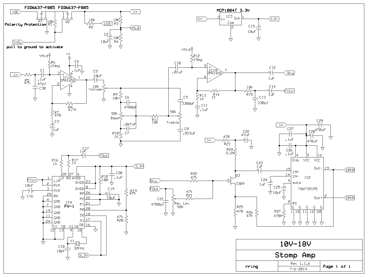
This design uses junk box 2N2222A or 2n3904 transistors. Its easy to build and offers excellent performance. Here is a preliminary schematic. It works well but I am still tweaking it. Look for revisions to follow.

A few quick notes:

It only uses bipolar transistors, and the antenna signal can be injected such that it is  isolated from the tank or directly to the tank through a small cap. The circuit can use a series resonant Clapp type topology or parallel tank. The clapp version reduces the effect of parasitics and provides very stable tuning. It also works really well with varactor tuning as the voltage  swing across the varactor is low. The series tank requires larger inductors for a given frequency then a traditional parallel tank. I am using 20uH(two crappy tiny molded inductors) and a 300pf variable to get in the 5-8Mhz range. You don’t need any tapped coils or tickler…etc – just about any inductor should work.

The parallel tank version  gives more tuning range for a given tank circuit. It may be a better topology..its hard to tell. You get more tuning range for small tuning caps and the the inductor will be smaller. You also eliminate the collector resistor which surely adds phase noise to the clapp version, when oscillating.

Depending on the tank coil you use and/or if you use a different supply voltage, you may need or want to adjust some of the resistor values. These are noted on the schematic. On the bright side, I have use wide range of values for most of these components and the circuit has still worked. It’s all about maximizing gain while still maintaining smooth regeneration.

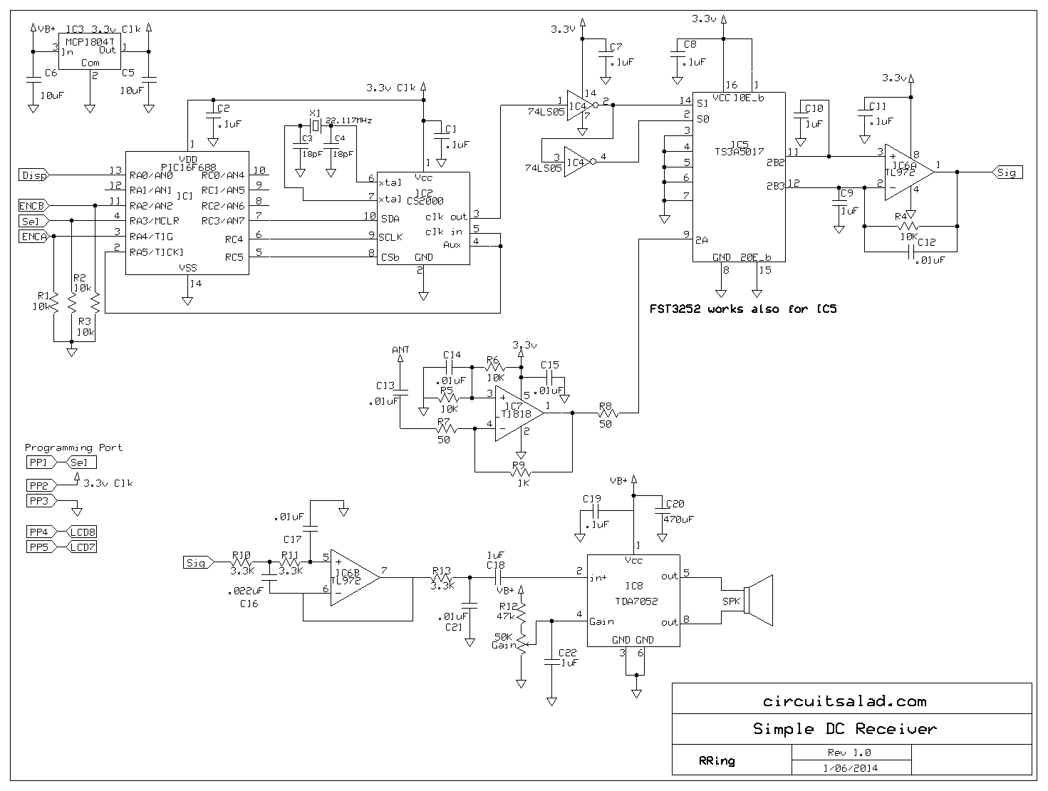
The darlington detector is a bipolar version of a “plate detector” where the the darlington is biased just at cusp of being turned on. It acts like a halfwave detector but with high Z and significant gain. You could use a FET but I thought it would be fun to only use junk-box type transistors. I am using 100k and 47k biasing resistors for the detector. The ratio is what matters so 1meg and 470k will work fine also.

In the schematic, I show the detector connected to L1 and C4 which make up the tank circuit for tuning. I also show a Q multiplier circuit separately which connects via the “QOut” signal to the tank circuit also. Its just another way to conceptualize a regenerative radio.

The transition from oscillation  is very smooth. Sensitivity is excellent. The circuit is simple.

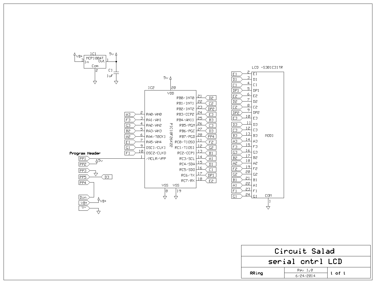
Schematic Diagram(modified TDA7052at circuit 07/01/2015)

2222A regen

Video demo showing smooth regeneration transition on a scope


PWM Phaser using PIC DDS LFO and 74HC4066 analog switches as synthetic resistors

I finally got this thing working well. I am using a TL5001 PWM chip  at 48 Khz to pulse width modulate analog switches in series with 10k resistors. The average resistance seen by the all pass filter circuits is proportional to the on time of the switches. For example is the switches are only on half the time, the average resistance is 20k instead of 10k. The advantages of this approach are that there are no critical adjustments, good dynamic range, and extremely linear resistance change in proportion to control voltage. The current draw is 25mA or so…not great but better than the 50mA I started with. The LFO is a DDS sine generator using a PIC micro controller. I will include a link to the code and a working hex file. I only use a sine wave output but the code can easily be modified to support numerous wave forms and frequency ranges. The  code for this project has been modified in two ways from the DDS code described in my other blog entries. I lowered the internal clock frequency to 8 MHz from 32Mhz(saves current) and reduced the output swing of the sine wave so it did not drive the PWM chip beyond 90% duty cycle.  Originally I just use the PWM directly from the PIC with no filtering but found this created noise artifacts, so I filter the output and drive a PWM chip. Typically, phaser circuits like this use high pass filter structures at the positive input, I chose to use low pass to help eliminate the switching noise from being introduced into the output. This worked well and eliminated the need for extensive filtering. The output is very clean

One thing that is very cool about this design is that it has variable sweep range instead of depth control. So the frequency range of sweep of the phasing notches can be adjusted starting at 100Hz or so all the way up to 5KHz.

Schematic:

pwm phaser


Demo

Link to code: https://www.adrive.com/public/mWSkFb/PWM%20phaser.zip

Another Quick Demo of my “No Tuned Circuit” Direct Conversion Radio

This is a video of me listening to radio Cairo in my basement while working on other projects. The slight drift from zero beat can be heard at the end. This is from the transmitter drifting… not the receiver. I know this because I have looked with a frequency counter and the receiver stability is within a fraction of a Hz. This is really the only drawback of this radio- that you have to zero beat AM. Still it works pretty well as is.

My next step is to go back to quadrature output again and build a simple DSP demodulator out of popcorn 12bit ADC’s and a PIC micro. This way I can listen to AM without zero beating the carrier. This is done by generating two outputs 90 deg out phase, squaring them, summing them and then taking the square root. This gives you the magnitude of the envelope of the carrier or the AM modulation.

New phaser with Homebrew 1×4 Vactrol and DDS LFO

I decided that I  should build a Phaser using my PIC DDS LFO. I designed a PWM version using CD4066 analog switches but this had issues. It just drew to much current and had some noise artifacts. I got it working but it became more complicated  than I liked. However, the design was easily modified to use a homemade vactrol. The vactrol uses four photcells glued together to make a square and then the LED is glued right in the center. The whole thing is then covered in a piece of heat shrink, electric tape or whatever.  Performance is excellent and the circuit is simple. Of course the DDS can be replaced by some other conventional LFO circuit. The main issue is operating the LDR’s in a good range to get even and adjustable notch sweep. With this design, the sweep is adjustable and you can even eliminate one notch by pushing its position sub audio. The sweep controls the level of illumination of the LDR’s and thereby adjusting the total range of phase shift. The LFO uses my PIC DDS circuit and generates a Sine wave envelope. The code can easily be changed to generate other wave forms. I am going to include a link to the a zip file containing all of my source code. This was all compiled using MikroC. The program is small enough to compile in the freeware version of MikroC or you can just use my compiled hex file.

More detail on the PIC DDS is available on this blog in earlier post.

Link to source code and  hex file:  http://www.filedropper.com/ldrphaserdds

Completed Phaser:

brainwash

Schematic:

LDR phaser

Etched Circuit Board:

etched phaser brd

Completed Board:

phaser board

Homebrew Vactrol:

quad vactrol

The Kool-Verb

This is a simple but nice sounding reverb based on the FV-1 dsp chip. Lots of low pass filtering gives a nice washy sound. You can adjust from a small room to a large hall.  The unit provides about a 75/25(dry) max reverb. Anything more than that is useless. Check out the stomp amp demo for how it sounds…same reverb, but just with just one fixed room setting.

The switch mode power supply keeps the current down to 30mA so you can use a battery if desired. You can use a linear regulator and it will work great, but then the current consumption doubles.

The schematic:

Koolverb

built into a 1590b case:

kool verb


The PWM Squeazal revisited

I have enjoyed my PW modulated compressor and decided to make a feedback(the original was feed forward) version with improved attack and shorter decay response. The result is excellent – I love this version. I use a Zetex current monitor IC as a full wave rectifier and this lets me really speed up the attack. So the response is super fast, very low noise, very low distortion, and very large dynamic range.


SchematicPWM COMP1_2_4

Link to design files:

https://www.adrive.com/public/PNQ67U/squeazal_design%20files.zip

The Stomp Amp- A Battery Powered 25 watt Stomp Box Amp

This is an idea I have had for a long time and I finally designed one. The results are excellent. The amp uses a surface mount car stereo  power amp IC and can produce 25 to 30 watts with a 16V-18V supply into a 4 ohm speaker. The circuit fits in a 1590bb enclosure and has Reverb, Bass, Treble and Gain controls. The tonal response is tailored for guitar in the OP amp stages, along with the James/Baxandall tone stack. The James/Baxandall is a versatile choice because it provides boost and cut. I find it a better choice then the “beef stew” fender tone stacks. Reverb is provided by means of an FV1 DSP IC. It can be omitted easily if desired. The Power amp IC is bonded to the case to provide heat sinking when it is cranked up. I used a piece of  1/2 inch copper pipe -reshaped to be the heat sink. As I have done with some of my earlier amplifiers, I have employed negative feedback from the speaker back to a discrete stage driving the final amplifier. This is a common practice in tube amps to flatten the tonal response of the output transformers and so it is unconventional to apply it here. I find it affects the over all sound in a pleasing manner. The amount of feedback is small and could be increased or removed (this will affect the bias of the JFET Q3) All of the signal chains are low impedance (except the input) and gain distribution is such that the amplifier is very low noise.  The amp powers up when the input is plugged in. The output is not ground referenced so the output jack is isolated from the case -(which is grounded via the heat sink). All you need is a tool battery or 12-18V power supply and a speaker cabinet and you can blast away. The mosfets used for polarity protection and power switching are just high current PMOS devices and not special – lots of other devices will work here. The op amp is a low noise type with a wide supply voltage range – others will work here also.

Things to consider when building:

The amp IC  I used was a surface mount version – and I flipped it upside so I could bond a heat sink to the ground. there is also a leaded version available

Decoupling is critical – especially for power amp – the double decoupling caps on the schematic are one set at each of two VCC pins on the power amp

Capacitors C3 and C11 weight the amplifier to tonally for guitar – these can be changed making both 10uF for example will work fine. If you want to use a Bass guitar make C3 at least 4.7 uF

The passive tone stack was chosen to attenuate gain so that the FV-1 would not be overloaded.  Other tone stacks can be substituted just keep this in mind if you use the FV-1


The Stomp Amp along with some other pedal designs of mine

stompandsink

IMG_20140915_144357473


Schematic Diagram

guitar_porta_rev1.1.6


Simplified switching mixer DC receiver uses no tuned circuits

This receiver is a simplified version of my quadrature sampling receiver. It  is simplified because it does not require the phasing filter section and also does not divide the LO by 4. This simplifies the local oscillator requirements significantly. The receiver uses a 2 pole low pass filter for selectivity and a TDA7052 audio amplifier. The CS2000 is a SPI controlled clock generator and is used for frequency generation and tuning, but any VFO, VXO  or any other stable frequency source will work. In this case, one of the extra inverter stages could be used as a linear amplifier to boost up the oscillator output if required(need a good squarewave). If this is done, the micro-controller can be eliminated. The input RF amplifier can also be eliminated if you are using an approximately 50 ohm resonant antenna. In this case the antenna would connect through C13 to pin 9 of IC5. If you do this – pin 9 must also be biased to 1/2 supply. This can be done with a couple of  4.7k  resistors connected in series from V+ to Gnd. The center  junction point will go to pin 9.

This receiver can receive AM but must be at zero beat(exactly tuned). The CS2000 has a resolution of 1Hz or so and is very stable – so the receiver work pretty well for AM. Unlike the phasing receiver this circuit cannot eliminate one of the side bands, but to be honest its not worth effort unless you want contest grade ham receiver performance.

In the video you can see I break out the power switch, audio gain, tuning encoder and display to a daughter board.

I designed the display to have very low spurious noise. The info on this is here:

https://circuitsalad.com/2014/07/31/very-low-power-3-digit-lcd-display-with-serial-control/

More info about how this circuit works can be found in this post, which is the quadrature version of this receiver.

https://circuitsalad.com/2013/12/30/my-phasing-receiver-is-a-success/

Schematic:

DC Receiver

Demo Video:

zip file of code: Filedropper is full of dumb ads but look for the “Download This File” button in middle of screen

http://www.filedropper.com/rcvrfirmware2

Very Low power 3 digit LCD Display with serial control

I had a need for a LCD display that consumed very little power and generated very little digital noise . You can buy LCD’s with driver chips but I have had great difficulty with these modules because they create excessive wide band noise.

To solve this problem, I made an LCD driver out of a 18F26K22 PIC micro-controller and a low cost static LCD display module. A static module requires more pins( a pin for every segment) but the drive logic is easier to implement. You cannot simply drive the the LCD segment high or low, as with a seven segment LED display. Once the capacitance of the display charges up, the segment contrast fades. The solution is to cycle a given segment on and off  at rate fast enough not to strobe(100Hz in my case).

In my design, the  display is driven by a four byte serial data packet which consists of: <startbyte>,<digit1>,<digit2>,<digit3> . The data bytes are sent as rs232 data at 9600 baud.

The startbyte is one of  three values(shown here in HEX): oxA0(no decimal point), 0xA1(decimal point 1st digit), 0xA2(decimal point 2nd digit). The valid data bytes are 0-9(non ASCII) and ASCII characters, “A”, “C”, “E”,”F”, “H”, and “P”. If you send any other values for a given digit, it will clear(blank the digit)

The module is clocked using the internal RC clock at 1Mhz and only draws 500uA when operating. It must be operated at greater than 4v or the LCD will be faint. If using a 3v supply, you can use a simple Dickson voltage doubler circuit to generate the supply voltage.

Picture of module(LCD covers the micro-controller):

LCDisplay

Demo Video: (Radio Receiver using the display module)

Schematic Diagram:

LCD_MOD_3Char

Link:   Zip File with ExpressPCB layout file and HEX file

http://bit.ly/1rDKMx1