When is A Capacitor not a Capacitor?

This is not a riddle but a painful reminder of  how un-ideal a capacitor can perform  in real world circuit conditions.  I measured the capacitance and Q factor for these capacitors shown below on a Agilent 4263B LCR meter, using 100Hz and 100Khz frequencies.

From left to right the capacitors in the picture are:

1000uF electrolytic,                     .01uF ceramic,                      10uF ceramic,                       .1uF tantalum

At 100Hz the results are as one might expect :   1007 uF, Q of 7     .014, Q of 100       8.6 uF , Q of 36       .104, Q of 80

The large electrolytic has a pretty low Q though indicating already at 100Hz its performance is starting to suffer

At 100Khz  things get really interesting : The 1000uF is now -.1 uF which is actually an inductor! The .01uF is .0098uF and the Q has gone down to 35. The nominal 10 uF(8.6) is now 8.2uF- not bad but the Q is down to 3. Finally the .1uF tantalum is now a .05uF with a Q of 1.2.

So even with this modest change in frequency, we can see capacitance starts to decrease as stray inductance becomes more of an effect. Also all of the capacitors start to become more lossy( low Q).

The bottom line here, especially with regard to decoupling, one large cap will not work well in most applications. One may have to use a combination of different type and value capacitors to achieve intended results.

PT2399 Design Updates

I have produced a PCB and built a new delay using the PCB and the original schematic. The results are gratifying. I did make a couple of minor adjustments.  The board is designed to fit in a 1590b stomp box. It draws 20mA so it works pretty well on a 9V battery.

R12 – changed from 33K to 39K

R2- changed from 56K to 47K

c19- changed from 2000pF to 2200pF

c16- from 247pF to 300pF

PCB Picture:

https://circuitsalad.com/wp-content/uploads/2012/09/img_4882.jpg

Video Demo Here:

Updated Schematic:

Tesla Coil – A Powerful Radio Transmitter with A Lousy Antenna!

I have tried to figure out what exactly a Tesla Coil was for years. I finally occurred to me that the best way to think of a Tesla Coil was as a very high power rf transmitter simply with a terrible antenna. The secondary is really just an ultra shortened 1/4 wave antenna – so short it can barely radiate RF at all. Ultimately the energy boils off the top of this antenna as the discharge us mad scientists know so well.

To prove my conception of a Tesla Coil: I built a class E amplifier that is powered from a simple half wave rectifier and 120VAC straight from the wall. A class E amplifier is simply a power mosfet switched on and off by a square wave drive (highly non linear all on or all off). The trick is to load the output with a slightly out of tune resonant circuit with respect to the frequency of the pulsing. By doing this, the voltage and current waveforms become 90 degrees out of phase. Since power is current times voltage, if they do not overlap (or very little) as in the case of a class E amplifier; no power is dissipated across the semiconductor switch and efficiency can approach 90+ percent. The draw back of such an amplifier is that it is narrow band and must be critically tuned.

A Tesla Coil is ideal as a load for such an amplifier. If you check out the schematic below you will see it is shockingly simple (pun intended). The schematic is incomplete in that I do not show the driver circuit. The driver is nothing special – just a mosfet driver IC (there are a million of them out there) and a couple of 555 timers to create a modulated (30Hz 20% duty cycle) 300KHz pulse source. I can also just use my  bench sine/square generator. The reason I modulate it at 30 Hz  it is twofold, one, to give the crackly long streamers and two, if I run in continuous mode the resonant caps will explode from over heating, also the secondary overheats and starts melting, catching on fire ( both of these events happened to me).

While the design is simple, tuning is challenging – if the current and voltage are ever in phase… forget it.  Get ready to blow some FETS!

Schematic: https://circuitsalad.com/wp-content/uploads/2012/09/class-e-tesla.gif

Pictures:

https://circuitsalad.com/wp-content/uploads/2012/09/img_48671.jpg

https://circuitsalad.com/wp-content/uploads/2012/09/img_48711.jpg

https://circuitsalad.com/wp-content/uploads/2012/09/img_48681.jpg

Video Link:

http://www.youtube.com/watch?v=tPK7-uS64IM&feature=player_detailpage

Alternate Analog Filter for PT2399 Delay

I am using a MAX7401 switchcap filter in my simple delay pedal, but this chip is expensive and not a common junk box part people have on hand. So here is an alterante choice – its only four pole (not 8 pole like the MAX7401) but it should work fine. I use an OPA1652 op amp but others could be used. The op amp needs to be rail to rail because of the 5 volt supply used. A TL072 will not work! I think using the PT2399 for the 1/2 supply ref and sharing the 5Volt supply is a good idea with regard to digital noise.

Schematic:

https://circuitsalad.com/wp-content/uploads/2012/09/alternate-delay-filter.gif

Filter Plot:

https://circuitsalad.com/wp-content/uploads/2012/09/analog-filter-response.gif

Using A PMOS FET as Reverse Polarity Protection

I fry a lot of electronics – so I like to include reverse polarity protection when I can. But there is a problem with using a traditional silicon diode, namely dropping .7 volts across the diode(more with high current). Consider that in an earlier post I described a 20 watt,  amp I designed. If this amplifier is drawing 1 amp, a standard silicon diode wastes .7 Watts or more!

A better choice is to use a PMOS FET as shown in the picture below:


The way it works is that the Gate is grounded and only when the SOURCE is at a higher potential than the GATE will the PMOS conduct across from Drain to Source. This only occurs when the supply voltage conducts across the internal substrate diode(Dinternal), energizing the SOURCE and allowing conduction. When the PMOS is turned on, the drop across the mosfet is only millivolts (depending on the mosfet specs), much less than a traditional diode.

How to Significantly Improve a Simple PT2399 Delay Circuit

Lots of great PT2399 designs out there….. I have tried a number different variations and have built what I consider a best performance design, using a compander, elaborate filters, etc. I have been frustrated as many builders out there are – that the PT2399 is so easy to use but that it just goes to crap with longer delay times! So I decided to work and experiment with different approaches to converge on a simple, yet well performing design. I am really happy with what I have come up with.

The design uses a discrete FET input buffer and uses one of the on board op amps as the wet/dry mixer. The dry signal always passes through and the effect is defeated by just opening the connection of the signal input to the delay chip. This allows “tails” or the echos to naturally decay even when the delay is bypassed. There are two features that make this circuit perform really well. One, the cap between pins 9,10 is made much larger than typical in other designs and the data sheet reference design and two, I use a 8 pole switch cap filter IC for the post delay aliasing filter. The larger cap provide significant increase in the delay output but the noise remains at the same level. I then attenuate the output in the wet dry mixer to the normal level this also downward expands the noise. The switch cap filter is really simple, requiring only one capacitor to set the corner freq from 1Hz to 5KHz. It is very easy to implement and has excellent performance. The total circuit rivals the simplest bare bones designs but approaches the performance of the more advanced circuits such as the PT80 delay.

Below are the schematic, a picture of a breadboarded prototype and some example audio of the prototype below, in use.

Updated Version in pedal form

moonchild solo

Schematic: https://circuitsalad.com/wp-content/uploads/2012/12/analog-delayschematic1.gif

Picture of Prototype:  https://circuitsalad.com/wp-content/uploads/2012/09/delay_proto.jpg

Sound Sample: https://circuitsalad.com/wp-content/uploads/2012/09/delay-demo.mp3

Enhanced Orange Squeezer type Compressor

This is my twist on the Orange Squeezer compressor. I use an h11M1F optofet instead of a JFET as a current controlled resistor (not voltage controlled). The signal chain is discrete FET and the control signal is generated from a ZETEX  ZXCT1041 current sensor – used for battery chargers. It is configured to act as a full wave precision rectifier. Unlike the Orange Squeezer you can adjust level and compression – it has all sorts of potential for mods. The  ZXCT1041 can be replace by an opamp such as the one I use for the peak detector, configured as a precision full wave diode(see op amp data sheet) – not much difference either way.

Schematic: https://circuitsalad.com/wp-content/uploads/2012/09/fet-compressor.gif

Picture: https://circuitsalad.com/wp-content/uploads/2012/09/img_4862.jpg

Sound Sample: https://circuitsalad.com/wp-content/uploads/2012/09/compressor-blues.mp3

recording starts with no compressor -> compressor on-> off->on->off-> ends with compressor on

UPDATE: 10/14/2012

I have noticed that at very low compression settings with high guitar input levels(>.5Volts) there can be some distortion. The Opto FET  I am using appears to have distortion that looks like crossover distortion with signals greater than 200mV. When compressing the signal across the OPTO FET decreases so that normally eliminates this issue but at low settings – this may be a problem. I am going to explore just using a linearized JFET in its place and or other solutions.

UPDATE:10/17/2012

By applying shunt shunt feedback from the Drain to the Gate of the first JFET stage of my compressor, I reduce VDS across the optofet  by a factor of 5! So with a input of 1 volt, the the VDS of the optofet is about 200mV worst case. Now it performs beautifully. The feedback consists of a 470k ohm resistor in series with a .1uF cap from drain to gate. Now the source must be bypassed with a 10uF cap – where before it was optional. The gain of the stage with this feedback is now about 4. What happens is that the feedback subtracts from the input at the optofet drain node greatly reducing the VDS across the voltage controlled resistor – while still providing gain.

Simple FET Overdrive Guitar Pedal

This is a really simple design for an overdrive pedal. My goal was very low noise, low power consumption and an overdriven amp type distortion sound. The circuit uses a very low noise OPA1652 to boost the input and control overdrive level. The signal then goes into a single voltage starved Jfet operated at 5 volts to create the distortion. The biasing of the Jfet is fairly critical, in order to make the distortion symmetrical. If other  Jfets are used, one might have to tweak the bias resistor values. The pedal is very low noise and provides signal boost – all the way to heavy distortion. What I like about it most is that the pedal is very responsive to playing dynamics, allowing for subtle all the way to crunch type distortion depending on how aggressive you play lines or chords.

In the schematic, Q1 and Q3 are generic PMOS and NMOS fets- nothing special here – many will work. The PMOS is used as  reverse polarity protection. The NMOS is for the LED activation. Also the 5v regulator can be anything – even a zener if you like.

Schematic:

https://circuitsalad.com/wp-content/uploads/2012/09/fet-overdrive1.gif

Pedal Pic:

https://circuitsalad.com/wp-content/uploads/2012/09/fet-overdrive.jpg

Sound Sample:

https://circuitsalad.com/wp-content/uploads/2012/09/overdrive-demo.mp3

20 Watt Battery Powered Guitar Amplifier Circuit


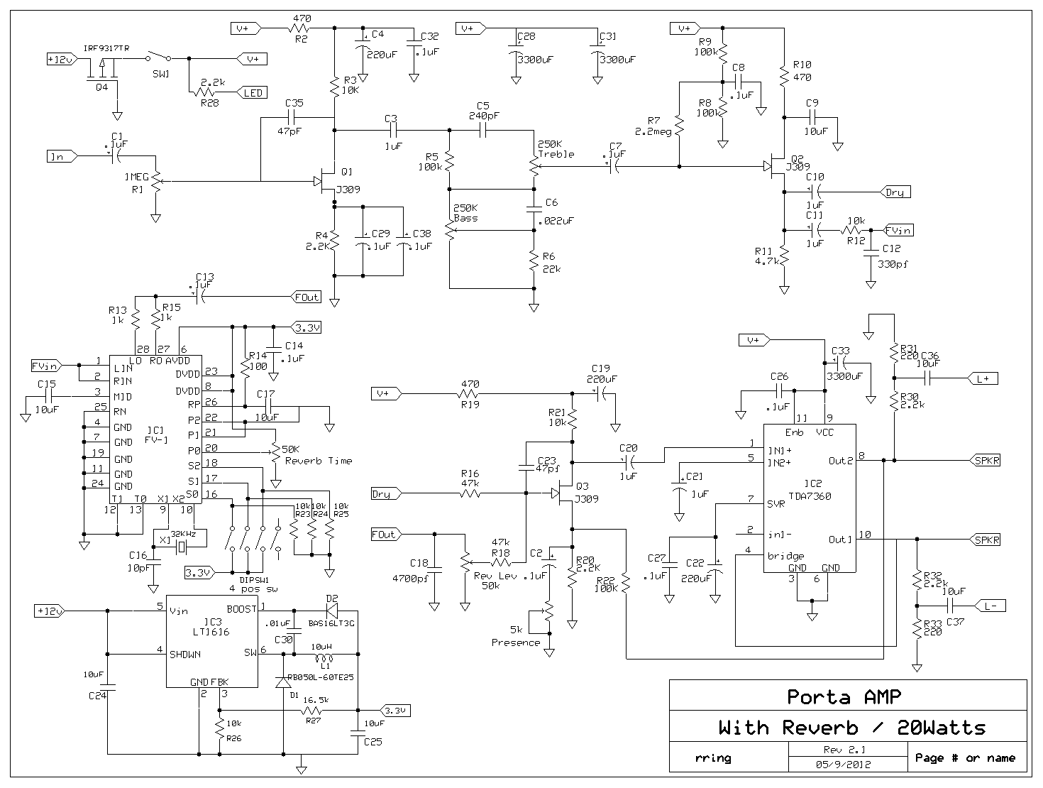
This is an amplifier I designed for busking and just so I could play crazy sounding stuff in the fields around my house here in Sandy Mush.  The design is tailored around some key criteria, namely; be able to provide 15 – 20 watts from a nominal 12 volt supply (10-16 volts), have a tube amp sound, reasonable simplicity and great sounding reverb. I am very pleased the final design. This is my primary practice amp now – mainly because I love the way it sounds and also I like seeing the bile drool out of the mouths of my mortified neighbors as I “rock out”.

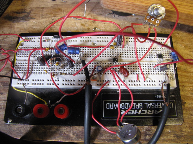
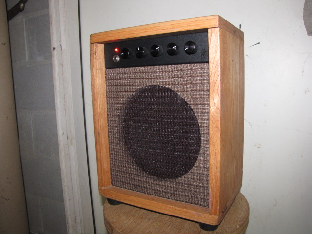
I am posting links to the original schematic and a version without the reverb – which simplifies the design a bit. I am also posting some pictures of the circuit board, a completed unit and some sound samples.

NOTE* Have updated design and thru-hole layout here: https://circuitsalad.com/2013/03/16/portable-battery-amp-thru-hole-version-schematic-and-layout-link/                                                                                                                                this new version uses a new final amp TDA7396 (TDA7360 discontinued)

Click Here To See and Hear:
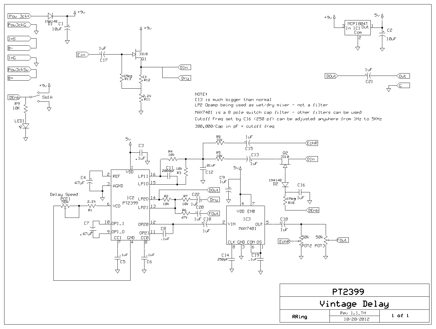
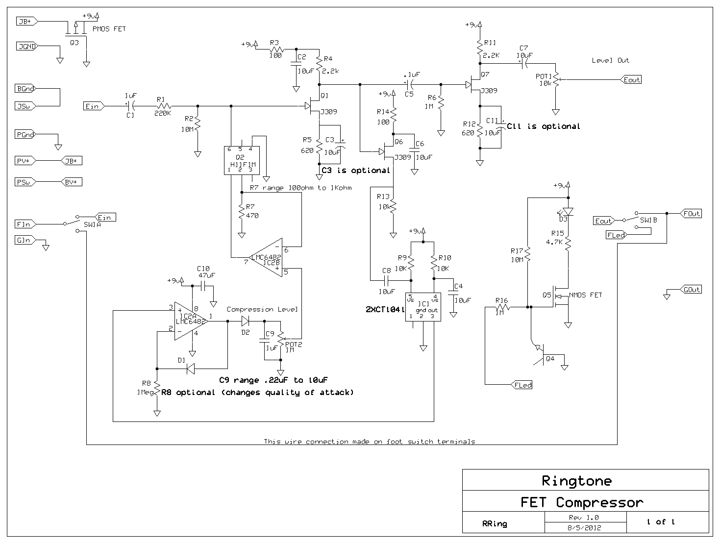
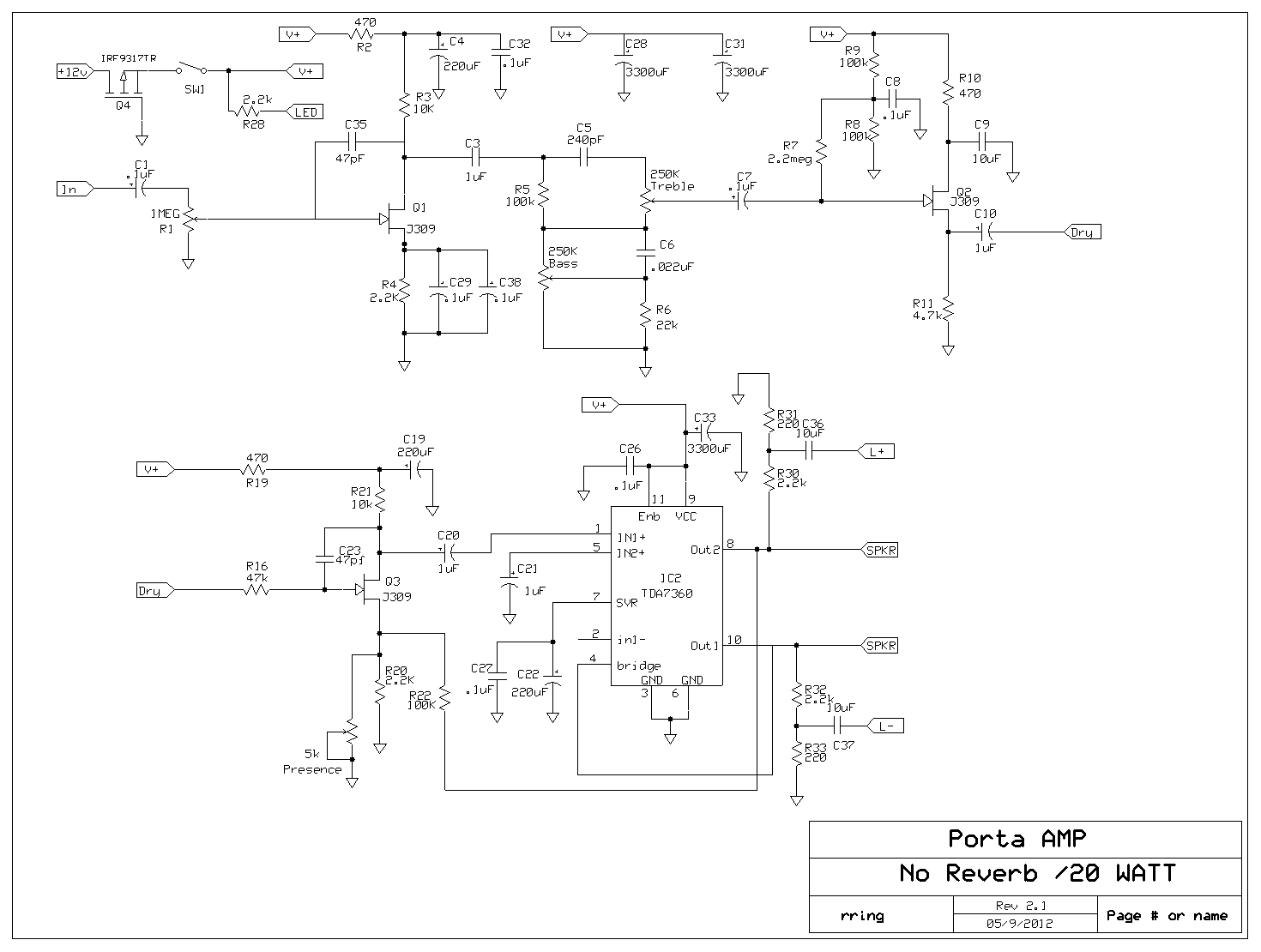
Schematics:

https://circuitsalad.com/wp-content/uploads/2012/08/portaamp.gif

https://circuitsalad.com/wp-content/uploads/2012/08/portaamp-no-reverb.gif

Pics:

https://circuitsalad.com/wp-content/uploads/2012/08/20-watt-battery-amp.jpg

https://circuitsalad.com/wp-content/uploads/2012/08/battery-amp-circuit-brd.jpg

Samples: recorded with DR1 pocket recorder about 2 feet away

 Neck pickup,  bass/treble middle setting – no reverb

https://circuitsalad.com/wp-content/uploads/2012/08/dry-blues.mp3

 Bridge pickup , bass/treble middle setting – small room reverb 1/3 depth

https://circuitsalad.com/wp-content/uploads/2012/08/not-fade-away_small-room.mp3

 Neck pickup,  bass/treble middle setting – large room reverb 1/3 depth

https://circuitsalad.com/wp-content/uploads/2012/08/large-room-reverb-noodle.mp3

Features:

Power – I used as the final amplifier a TDA7360 car stereo amplifier in bridged mode. This amp sounds great and can provide 20 + watts through 4 ohms with a 14v supply. Some may shuddered in horror at the thought of this used for a guitar amp, but it really works well and is reasonably efficient, requiring only the circuit board ground plane as heat sinking. I use a small lead/acid gel cel to power this amp but also have used drill batteries and a computer wall wart, etc.

Tube Sound – To achieve a tube like sound I used a classic fender type tone stack, discrete signal chain using jfets (up to the power amp) and negative feedback from the speaker to the final preamp stage. If you look at the circuit, you can see that basically all of the active devices could be replaced with tubes and the TDA7360 with a couple of output tubes and a transformer. The negative feedback from the speaker is a classic technique in tube amps and applied here, has a noticeable effect on the sound.

Simplicity – I set a limit on physical size and number of knobs which forced me to keep it simple.

Reverb – I thought seriously about integrating a spring reverb, but went with a DSP circuit, the FV- 1  chip, instead. This IC provides a number of reverbs and other effects which are selectable via switches(jumpers). It is easy to use and I was able to color the reverb with filtering to my taste. It is essentially an effects  unit on a chip. I very pleased with its performance. The reverb has both room size and depth control, and provides all kinds of variation.

Design Notes: There is flexibility in this design – you don’t have to use a switch mode 3.3v power supply for the FV-1 like I did – you could just use a linear regulator. I use a PMOS FET as a  NO VOLTAGE DROP protection diode. This could also be omitted. I hate to lose .7 volts with a regular diode though – so I recommend the PMOS approach. The choice of JFET was based on what I had kick’n around – nothing else. I also tried it using LND150’s with similar results. My tone stack is nothing special and many other variations could be used. The volume control at the very front may seem odd. In fact, at very low volume settings, there is treble roll off because of stray capacitance of the POT. The reason I did it was to maximize headroom of the preamp stages and simplicity.  This is a design choice that merits a second look. The amount negative feedback from the final to the driver stage is adjustable or can be omitted. A high-end treble control (presence) is realised by bypassing this feedback for very high frequency. This too can be omitted.

For the speaker I used a $22 Jensen 8″ MOD. I highly recommend this speaker – its cheap and sounds perfect.