
I have produced a PCB and built a new delay using the PCB and the original schematic. The results are gratifying. I did make a couple of minor adjustments. The board is designed to fit in a 1590b stomp box. It draws 20mA so it works pretty well on a 9V battery.
R12 – changed from 33K to 39K
R2- changed from 56K to 47K
c19- changed from 2000pF to 2200pF
c16- from 247pF to 300pF
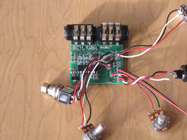
PCB Picture:
https://circuitsalad.com/wp-content/uploads/2012/09/img_4882.jpg
Video Demo Here:
Updated Schematic:


Can you post shematic for it. PCB does not have electrolytic capacitors (I can see only one or two) from the previous one, it was something changed.
Not sure I understand your issue??? but I will post the schematic in the entry you have referenced.
Do you know where I can get the MAX7410 chip?
Do you have any equivalent part number for this chip?
Thank you very much
the 7401 and the 7410 will work(I think there are other similar parts also made by maxim that would work).I get mine from Digikey and or Mouser
Ray,
It’s Kirk. I’ve rounded up the boards and most of the parts for the surface-mount version. I appreciate the BOM you provided. I had one more question. I was comparing the picture (https://circuitsaladdotcom.files.wordpress.com/2012/09/img_4882.jpg), the board and the schematic and can’t quite figure out what the component is that’s connected to JSw/J-/J+. It’s the one hanging off to the left of the photo. It sort of looks like a fuse holder or lamp base. Can you clue me in?
Thanks,
-Kirk
hey there
that is a 2.1mm x 5.5mm circular power jack..which is standard for guitar pedals. the tip is wired negative so that the switch leg can be used to bypass the battery when using a power adaptor. if you connect the battery ground to the switch leg(normally closed to the jack tip) a ground path for the battery only occurs when there is no plug inserted into the jack. the shell gets the positive connection. The battery ground is connected using a stereo input jack, where a mono 1/4 inch plug shorts the inner stereo connection(ring) to ground so the ring(not tip) becomes the ground path to the circuit only when a plug is inserted into the jack. If I can help you let me know…I want you to succeed in your efforts
Almost done, I got side tracked with work and all that nonsense. I was down to soldering in the last component, the LDO. I mistakenly ordered 2.5 volt LDOs, waiting for the correct ones to come in now. Hey, I’m working off the original Rev 1.0 (8/5/2012) schematic. Would you by any chance have the gif of that? I can’t find it on your site now and I’d like to have a soft copy for my archives; I only have a printed copy of it.
Thanks,
-Kirk
I WILL LOOK AND GET BACK WITH YOU
here is a download link to a zip file containing everything I have for the delay
https://www.adrive.com/public/vgprUq/Delay.zip
Ray,
The schematic I was looking for is in the zip file. It’s the one named Analog Delay Surface Mount_08_05_12.bmp.
Thanks!
-Kirk
cool let me know how it goes or if you have any trouble with it.
My first unit is finished and it works like a charm! I gave it to my guitarist grandson, he loves it. One down and three more to box up. I had bought two of the Hammond boxes but trashed the first one trying to figure out where in the box to place the board. I appreciate your encouragement and help in putting this project together. It was a good project to learn how to built with SMDs. I bought a fine tipped 12W Weller, which proved to be just the right size to avoid going scorched Earth on the circuit boards.
so great! I have templates for hole patterns…etc.. I should have sent you that info I guess!