
By applying shunt shunt feedback from the Drain to the Gate of the first JFET stage of my compressor, I reduce VDS across the optofet by a factor of 5! So with a input of 1 volt, the the VDS of the optofet is about 200mV worst case. Now it performs beautifully. The feedback consists of a 470k ohm resistor in series with a .1uF cap from drain to gate. Now the source must be bypassed with a 10uF cap – where before it was optional. The gain of the stage with this feedback is now about 4. What happens is that the feedback subtracts from the input at the optofet drain node greatly reducing the VDS across the voltage controlled resistor – while still providing gain.
Audio Electronics
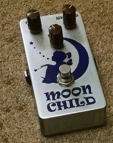
Get the Simple FET distortion PCB layout here
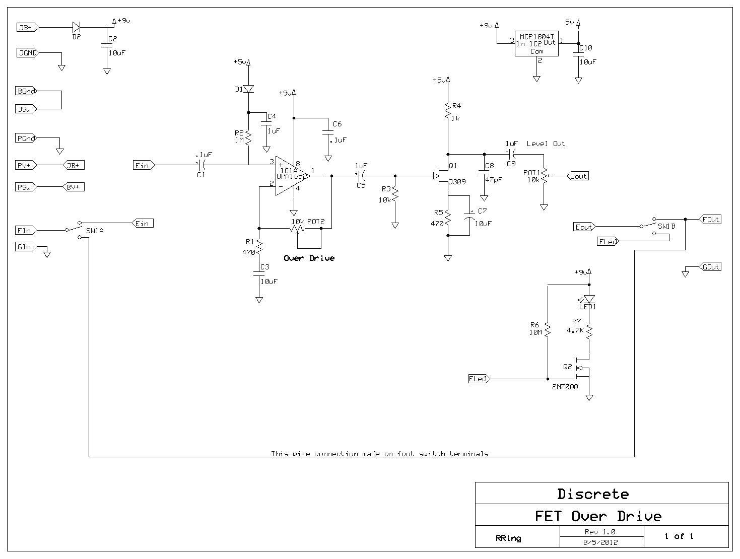
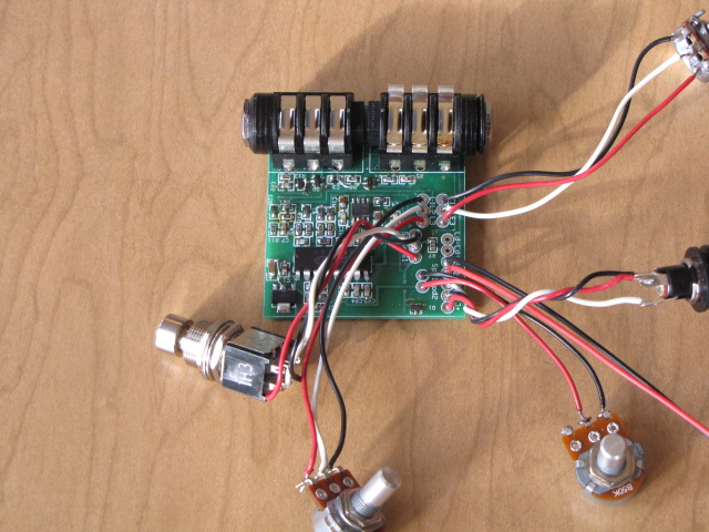
Here is the simple FET distortion layout for through hole components. The schematic has minor changes to match this layout. So get this new schematic also. The layout is done with the expresspcb design tool. You can download their free CAD tool online. the layout can easily be modified or just ordered through expresspcb (lowest cost small quantity option is for 3 boards in three days for $60.00). The board is small and designed to easily fit in a 1590B box. I will add a parts list shortly.
Go to this link for .pcb file:
use slow download speed(free)
http://www.fileswap.com/dl/pPTjbxAOm/
new schematic:
https://circuitsalad.com/wp-content/uploads/2012/10/fet-overdrive_throughhole.gif
Going to post Fet Distortion PCB Layout this Week
Check out the video demo of it in action:
http://www.youtube.com/watch?v=1c3BYFAABAw&feature=player_detailpage
Further Simplification of the Enhanced Orange Squeezer Compressor
It occurred to me that if one is willing to sacrifice some flexibility in the decay length of my compressor design; that it can be simplified by removing the source follower and the Zetex current sensor. What this means is that the control voltage is only half wave rectified instead of full wave, but if you just increase the filter cap – the circuit should still work fine. The trade-off is that you get limited to longer decay times only, but for most guitar applications this is fine. I have not verified this circuit but I will do this soon. I am confident it will work well. Removing these parts may make it more attractive to the DIY builder.
New Schematic:
https://circuitsalad.com/wp-content/uploads/2012/09/compressor3.gif
PT2399 Delay is Complete
Yes its ugly – but it works great!

Check out the videos below. I have pooped out a slap back demo. You can get a really great 50’s tape echo sound
slap back
Pedal and Amp demo videos to be posted
I have been building a lot of guitar electronics these days … and more to come I hope! Having said that, I think it is important to show how they can be used in real music and how well DIY designs can perform as compared to commercial products. My first demo is of my portable busking amp and my FET discrete signal chain compressor. This demo represents a classic jazz sound using the compressor to understate all of elaborate grips on the guitar and make the lines very smooth sounding even with heavy down strokes.
check it out at:
more demos to come shortly!
PT2399 Design Updates
I have produced a PCB and built a new delay using the PCB and the original schematic. The results are gratifying. I did make a couple of minor adjustments. The board is designed to fit in a 1590b stomp box. It draws 20mA so it works pretty well on a 9V battery.
R12 – changed from 33K to 39K
R2- changed from 56K to 47K
c19- changed from 2000pF to 2200pF
c16- from 247pF to 300pF
PCB Picture:
https://circuitsalad.com/wp-content/uploads/2012/09/img_4882.jpg
Video Demo Here:
Updated Schematic:

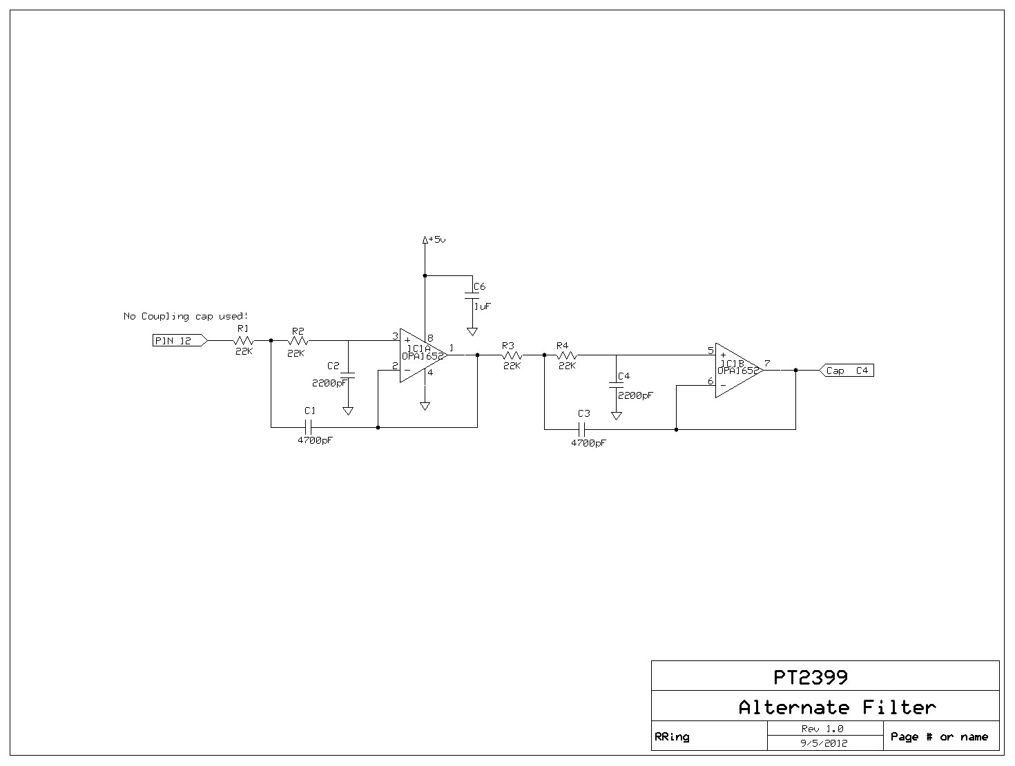
Alternate Analog Filter for PT2399 Delay
I am using a MAX7401 switchcap filter in my simple delay pedal, but this chip is expensive and not a common junk box part people have on hand. So here is an alterante choice – its only four pole (not 8 pole like the MAX7401) but it should work fine. I use an OPA1652 op amp but others could be used. The op amp needs to be rail to rail because of the 5 volt supply used. A TL072 will not work! I think using the PT2399 for the 1/2 supply ref and sharing the 5Volt supply is a good idea with regard to digital noise.
Schematic:
https://circuitsalad.com/wp-content/uploads/2012/09/alternate-delay-filter.gif
Filter Plot:
https://circuitsalad.com/wp-content/uploads/2012/09/analog-filter-response.gif
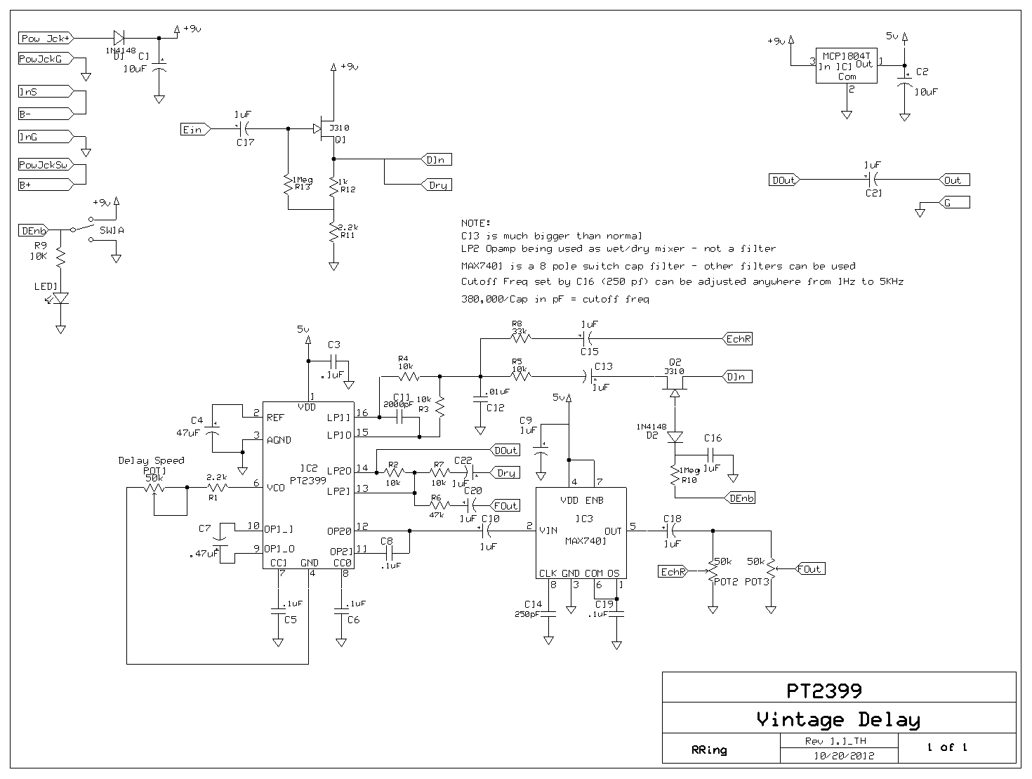
How to Significantly Improve a Simple PT2399 Delay Circuit
Lots of great PT2399 designs out there….. I have tried a number different variations and have built what I consider a best performance design, using a compander, elaborate filters, etc. I have been frustrated as many builders out there are – that the PT2399 is so easy to use but that it just goes to crap with longer delay times! So I decided to work and experiment with different approaches to converge on a simple, yet well performing design. I am really happy with what I have come up with.
The design uses a discrete FET input buffer and uses one of the on board op amps as the wet/dry mixer. The dry signal always passes through and the effect is defeated by just opening the connection of the signal input to the delay chip. This allows “tails” or the echos to naturally decay even when the delay is bypassed. There are two features that make this circuit perform really well. One, the cap between pins 9,10 is made much larger than typical in other designs and the data sheet reference design and two, I use a 8 pole switch cap filter IC for the post delay aliasing filter. The larger cap provide significant increase in the delay output but the noise remains at the same level. I then attenuate the output in the wet dry mixer to the normal level this also downward expands the noise. The switch cap filter is really simple, requiring only one capacitor to set the corner freq from 1Hz to 5KHz. It is very easy to implement and has excellent performance. The total circuit rivals the simplest bare bones designs but approaches the performance of the more advanced circuits such as the PT80 delay.
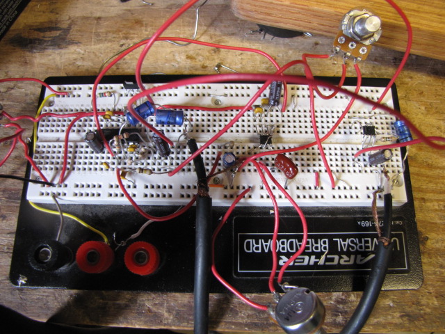
Below are the schematic, a picture of a breadboarded prototype and some example audio of the prototype below, in use.
Updated Version in pedal form
Schematic: https://circuitsalad.com/wp-content/uploads/2012/12/analog-delayschematic1.gif
Picture of Prototype: https://circuitsalad.com/wp-content/uploads/2012/09/delay_proto.jpg
Sound Sample: https://circuitsalad.com/wp-content/uploads/2012/09/delay-demo.mp3
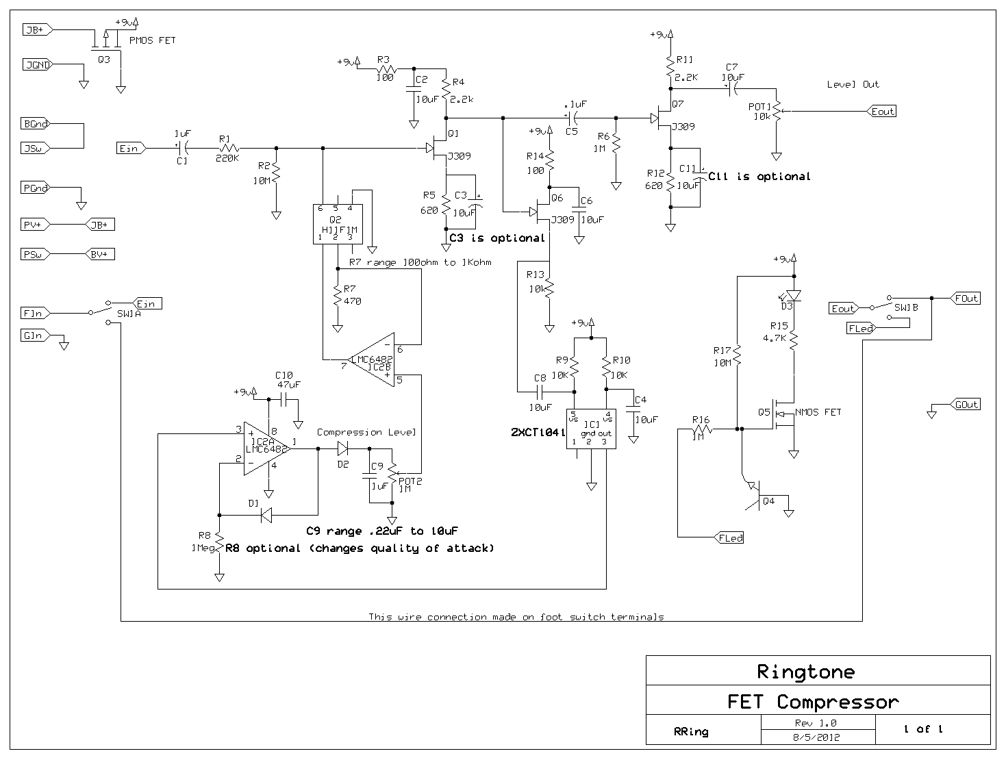
Enhanced Orange Squeezer type Compressor
This is my twist on the Orange Squeezer compressor. I use an h11M1F optofet instead of a JFET as a current controlled resistor (not voltage controlled). The signal chain is discrete FET and the control signal is generated from a ZETEX ZXCT1041 current sensor – used for battery chargers. It is configured to act as a full wave precision rectifier. Unlike the Orange Squeezer you can adjust level and compression – it has all sorts of potential for mods. The ZXCT1041 can be replace by an opamp such as the one I use for the peak detector, configured as a precision full wave diode(see op amp data sheet) – not much difference either way.
Schematic: https://circuitsalad.com/wp-content/uploads/2012/09/fet-compressor.gif
Picture: https://circuitsalad.com/wp-content/uploads/2012/09/img_4862.jpg
Sound Sample: https://circuitsalad.com/wp-content/uploads/2012/09/compressor-blues.mp3
recording starts with no compressor -> compressor on-> off->on->off-> ends with compressor on
UPDATE: 10/14/2012
I have noticed that at very low compression settings with high guitar input levels(>.5Volts) there can be some distortion. The Opto FET I am using appears to have distortion that looks like crossover distortion with signals greater than 200mV. When compressing the signal across the OPTO FET decreases so that normally eliminates this issue but at low settings – this may be a problem. I am going to explore just using a linearized JFET in its place and or other solutions.
UPDATE:10/17/2012
By applying shunt shunt feedback from the Drain to the Gate of the first JFET stage of my compressor, I reduce VDS across the optofet by a factor of 5! So with a input of 1 volt, the the VDS of the optofet is about 200mV worst case. Now it performs beautifully. The feedback consists of a 470k ohm resistor in series with a .1uF cap from drain to gate. Now the source must be bypassed with a 10uF cap – where before it was optional. The gain of the stage with this feedback is now about 4. What happens is that the feedback subtracts from the input at the optofet drain node greatly reducing the VDS across the voltage controlled resistor – while still providing gain.
