Slightly improved code for PIC DDS

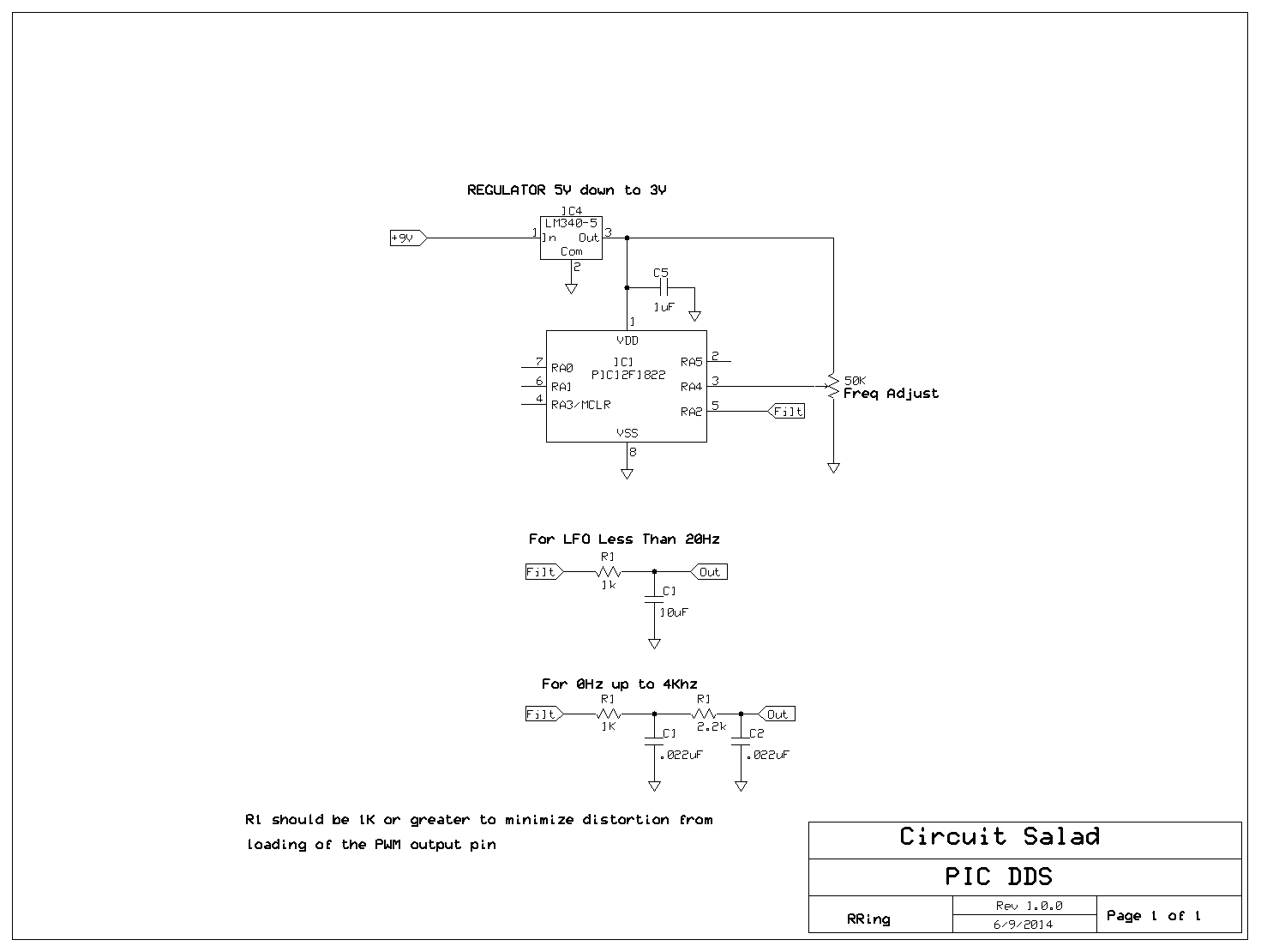
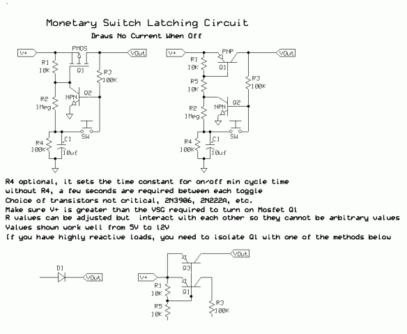
I realized my original code was delaying the PWM loop some because it was waiting on a ADC read before finishing the loop. In the code below, the ADC read is started and read the next time around. Then the next time is started again, this eliminates the delay of waiting on the ADC.


#define ADCStart ADCON0.b1 = 1 //set this bit to begin ADC conversion
//////////////////////////////////////////////////////////////////////////////
const unsigned char sine[256] =
{// sine wave 8 bit resolution scaled to 90% max val
131,132,135,137,140,143,146,149,152,155,157,160,163,166,168,171,
174,176,179,181,184,186,189,191,194,196,198,200,202,205,207,209,
211,212,214,216,218,219,221,223,224,226,227,228,229,231,232,233,
234,234,235,236,237,237,238,238,239,239,239,239,240,240,240,239,
239,239,239,238,238,237,237,236,236,235,234,233,232,231,230,229,
227,226,225,223,222,220,219,217,216,214,212,210,208,206,204,202,
200,198,196,194,192,189,187,185,182,180,177,175,173,170,167,165,
162,160,157,154,152,149,146,144,141,138,135,133,130,127,124,122,
119,116,113,111,108,105,103,100, 97, 95, 92, 89, 87, 84, 82, 79,
77, 74, 72, 69, 67, 64, 62, 60, 58, 55, 53, 51, 49, 47, 45, 43,
41, 39, 37, 36, 34, 32, 31, 29, 28, 26, 25, 24, 22, 21, 20, 19,
18, 17, 16, 15, 15, 14, 13, 13, 12, 12, 12, 11, 11, 11, 11, 11,
11, 11, 11, 12, 12, 12, 13, 14, 14, 15, 16, 16, 17, 18, 19, 21,
22, 23, 24, 26, 27, 29, 30, 32, 33, 35, 37, 39, 41, 43, 45, 47,
49, 51, 53, 56, 58, 60, 63, 65, 68, 70, 73, 75, 78, 81, 83, 86,
89, 92, 94, 97, 100,103,106,108,111,114,117,120,123,126,129,130};
////////////////////////////////Global variable here//////////////////////////////////////////////
long PhaseAccum;//phase accumilator generates the cycle rate for lookup table
//loading therby changing frequency. The MSbyte is used to provide the byte address
//of the look up table value to be used.
long PhaseShift;//value added to PhaseAccum every PWM cycle. This makes the waveform
//lookup faster or slower – which changes frequency.
////////////////////////////////////////////////////////////////////////////////////////////
////////////////////////////////PIC Config routine here////////////////////////////////////
void Init_Main(){
//PIC12F1822 specific config
OPTION_REG = 0b10000000; // disable internal pull ups
OSCCON = 0b11110000; //8MHz clk //32Mhz pll
TRISA = 0b00011000; // configure IO/a2d(gpio0) and mclr set as inputs
T2CON = 0b00000100;// TMR2 ON, postscale 1:1, prescale 1:1
PR2 = (0x50);// sets PWM rate to approx 98.5KHz with 32Mhz internal oscillator
CCP1CON = 0b00001111;// CCP1 ON, and set to simple PWM mode
PhaseShift = 0x00FFFFFF;//frequency values loaded into
ANSELA = 0b00010000; //select RA4 as A2D input 32Mhz clk
ADCON0 = 0b00001101; // configure ADC
ADCON1 = 0b00100000; // configure ADC
}
////////////////////////////main program loop here/////////////////////////////////
void main() {
Init_Main();//configue part
while(1){ //alway do this
while(!PIR1.TMR2IF);// wait for TMR2 cycle to restart
CCPR1L = (sine[((char *)&PhaseAccum)[3]]) >> 2;// load MSbits 7-2 duty cycle value into CCPRIL
CCP1CON ^=((sine[((char *)&PhaseAccum)[3]]) & 0x03) << 4;// load in bits 1-0 into 5 and 4 of CCP1CON
//////duty cycle value byte is now loaded for next cycle comming//////
if(PIR1.ADIF == 0)ADCStart; //start ADC here to get value into PhaseShift to change Freq
//will have to go around the loop one time before ready flag is high
if(PIR1.ADIF){ //if ADC read complete load values and clear flag
((char *)&PhaseShift)[1] = ADRESL; //load ADRESL into PhaseShift
((char *)&PhaseShift)[2] = ADRESH; //load ADRESH into PhaseShift
PIR1.ADIF = 0;//clear flag so next time ADC can run
}
PhaseAccum = PhaseAccum + ((PhaseShift << 5) + 1); //move PhaseAccum through waveform values
//”<<5″ can be more or less and sets the frequency sweep range
// the +1 is just so there is never 0;
porta.b0 = ((char *)&PhaseAccum)[3].b7;
PIR1.TMR2IF = 0; // clear TMR2 int flag
}
}

DDS audio generator made from PIC Microcontroller

I needed a sine wave generator and I didn’t want a whole lot of parts……. so I thought I would try making a Direct Digital Synthesizer out of a cheapo 8 pin micro controller.

I chose a 12F1822 PIC, but any micro with a PWM generator and an ADC will work.

A number of AVR and Microchip products are available. The 12f683 or the ATTINY85  are other devices that meet the basic  requirement. If using an AVR the code will have to changed but you can get the basic idea from the PIC implementation. If  you use another PIC, the code may need some minor tweaks , such as the pin assignments and/or the config register settings.

I settled on the  12f1822 for the following reasons: its cheap, its small, my C compiler supports it, it has an internal clk that runs up to 32MHz – which allows for 8 bit PWM at greater than 100kHz, which makes filtering the output trivial.  Also it is very power efficient.

The way DDS works  is by cycling through a look up table of values representing a sine wave(or any other wave form you choose… a triangle for example). These values range from 0-255 (8bit) and there are 256 values in  the table. Each value is loaded into a PWM generator in succession which varies the duty cycle of a roughly 100KHz PWM signal. The faster you  cycle through the values, the higher the frequency is generated.

I don’t want to explain all the details of how  DDS works- so go here to learn more about DDS:

Click to access MT-085.pdf

Here are the basics of my design:

I use the 10 bit ADC input to read a voltage of a POT and convert this to a number from 0 -1024. I use the PWM generator as a DAC to reproduce the sampled analog wave form. Then there is a simple filter to remove the high frequency artifacts caused by the 100Khz PWM signal. Every cycle of the PWM generator’s overflow flag – I add the value of the ADC to a 32 bit register which acts as a phase accumulator. The most significant byte of the phase accumulator is loaded as the address for the look up table value and as this value increments every cycle, a new value is loaded. If a smaller value is loaded into the phase accumulator, the frequency is lower. With a larger number loaded every cycle the frequency increases. The frequency resolution is given by 1/  (PWM period/2^32). This gives resolution less than a milli Hertz! The ADC value can be scaled as needed to get you in the frequency range of interest.

A note about my lookup table. The PWM generator will create distortion if the look up table values are not naturalized. This is because as the look up values are going up and down they should shift from when the off time occurs(either before the on time or after). So if you just generate the sine values they will work but not as well as they could. The solution is to naturalize the look up values. Which is to say shift them slightly. This process and how I did it is discussed here:

http://www.romanblack.com/onesec/Sine1kHz.htm

Also I scaled my sinewave to 90% of max and shifted it up 5%.  This makes it so that the PWM has no values to close to the extreme edges of its range. Also the output is from 1-4 volts instead of going all the way down to 0 volts. This way a single supply active filter can be employed.

Originally, I used a 12f683 PIC running at 8Mhz but could only support 20KHz PWM at 8bit resolution. The circuit worked but made it harder to filter the output and limited the frequency range to about 1Khz. the part I  used the 12f1822 has an internal clk that works up to 32 MHz. This allows a much faster PWM rate. Now I can get anywhere from .00005Hz to 5Khz output with a simple filter.

You can use an external crystal and get a more accurate and stable output, but the internal oscillator works pretty well. The harmonics are all 40db or more down from the fundamental.

Video demo:

Schematic:

C CODE: (compiled with MikroC ) will compile on freeware version with room to spare

Note!!!!! There is new code and is available here: https://circuitsalad.com/2014/06/13/slightly-improved-code-for-pic-dds/

#define ADCStart ADCON0.b1 = 1 //set this bit to begin ADC conversion
//////////////////////////////////////////////////////////////////////////////
const unsigned char sine[256] =
{// sine wave 8 bit resolution scaled to 90% max val
131,132,135,137,140,143,146,149,152,155,157,160,163,166,168,171,
174,176,179,181,184,186,189,191,194,196,198,200,202,205,207,209,
211,212,214,216,218,219,221,223,224,226,227,228,229,231,232,233,
234,234,235,236,237,237,238,238,239,239,239,239,240,240,240,239,
239,239,239,238,238,237,237,236,236,235,234,233,232,231,230,229,
227,226,225,223,222,220,219,217,216,214,212,210,208,206,204,202,
200,198,196,194,192,189,187,185,182,180,177,175,173,170,167,165,
162,160,157,154,152,149,146,144,141,138,135,133,130,127,124,122,
119,116,113,111,108,105,103,100, 97, 95, 92, 89, 87, 84, 82, 79,
77, 74, 72, 69, 67, 64, 62, 60, 58, 55, 53, 51, 49, 47, 45, 43,
41, 39, 37, 36, 34, 32, 31, 29, 28, 26, 25, 24, 22, 21, 20, 19,
18, 17, 16, 15, 15, 14, 13, 13, 12, 12, 12, 11, 11, 11, 11, 11,
11, 11, 11, 12, 12, 12, 13, 14, 14, 15, 16, 16, 17, 18, 19, 21,
22, 23, 24, 26, 27, 29, 30, 32, 33, 35, 37, 39, 41, 43, 45, 47,
49, 51, 53, 56, 58, 60, 63, 65, 68, 70, 73, 75, 78, 81, 83, 86,
89, 92, 94, 97, 100,103,106,108,111,114,117,120,123,126,129,130};
////////////////////////////////Global variable here//////////////////////////////////////////////
long PhaseAccum;//phase accumilator generates the cycle rate for lookup table
//loading therby changing frequency. The MSbyte is used to provide the byte address
//of the look up table value to be used.
long PhaseShift;//value added to PhaseAccum every PWM cycle. This makes the waveform
//lookup faster or slower – which changes frequency.
////////////////////////////////////////////////////////////////////////////////////////////
void ADCRead(){
ADCStart; //start ADC conversion
while(ADCON0.b1); //wait till done
((char *)&PhaseShift)[1] = ADRESL; //load ADRESL into PhaseShift
((char *)&PhaseShift)[2] = ADRESH; //load ADRESH into PhaseShift
}
////////////////////////////////PIC Config routine here////////////////////////////////////
void Init_Main(){
//PIC12F1822 specific config
OPTION_REG = 0b10000000; // disable internal pull ups
OSCCON = 0b11110000; //8MHz clk //32Mhz pll
TRISA = 0b00011000; // configure IO/a2d(gpio0) and mclr set as inputs
T2CON = 0b00000100;// TMR2 ON, postscale 1:1, prescale 1:1
PR2 = (0x50);// sets PWM rate to approx 98.5KHz with 32Mhz internal oscillator
CCP1CON = 0b00001111;// CCP1 ON, and set to simple PWM mode
PhaseShift = 0x00000000;//frequency values loaded into
ANSELA = 0b00010000; //select RA4 as A2D input 32Mhz clk
ADCON0 = 0b00001101; // configure ADC
ADCON1 = 0b00100000; // configure ADC
}
////////////////////////////main program loop here/////////////////////////////////
void main() {
Init_Main();//configure part
while(1){ //alway do this
while(!PIR1.TMR2IF);// wait for TMR2 cycle to restart
CCPR1L = (sine[((char *)&PhaseAccum)[3]]) >> 2;// load MSbits 7-2 duty cycle value into CCPRIL
CCP1CON ^=((sine[((char *)&PhaseAccum)[3]]) & 0x03) << 4;// load in bits 1-0 into 5 and 4 of CCP1CON
//////duty cycle value byte is now loaded for next cycle comming//////
ADCRead(); //read ADC here to get value into PhaseShift to change Freq
PhaseAccum = PhaseAccum + ((PhaseShift << 5) + 1); //move PhaseAccum through waveform values
//”<<5″ can be more or less and sets the frequency sweep range
// the +1 is just so there is never 0;
PIR1.TMR2IF = 0; // clear TMR2 int flag
}
}

Minimized implementation of the Tube Screamer

The Tube Screamer is a classic all around great sounding distortion, even though the stock circuit is not very complex, by eliminating the JFET bypass switching and utilizing true bypass you eliminate quite a few parts. Even more, you can eliminate the input and output follower stages a number of coupling caps and bias resistors. With just one op amp and less than 25 parts, you can make a tube screamer that sounds just  great. In my implementation, I changed some values in the filter section to suit my taste and on the first stage I used BAT46 shottky diodes. These diodes have substantial reverse leakage- so you have to lower the impedance of the feedback pot and resistor that controls the the drive gain. That is why I used a 50k pot and 100 ohm resistor. I used the shottky because they start to clip much sooner and you can get a really insane amount of overdrive. Regular silicon diodes work just fine. The original stock values can be used and can be found on the web.


Schematic:


Demo (coming soon)

A Simple LDR Envelope Filter that is just delightful

I designed  a low pass type envelope filter using a Fliege filter topology . The result was a really easy to build filter that provides1st order low pass ..all the way up to 2nd order low pass with extreme bandpass peaked low pass(high Q, resonance…etc). I really like this pedal.

drcream_2

Demo Sound Clips:

Short attack, max intensity:

Mid Attack, low intensity:

Long attack, high intensity:

This filter topology has some nice features, such as:

Fixed stable gain of two in the pass band, regardless of Q

Highly adjustable Q

Uses only two op amps

Low parts count in general

Well suited for single supply operation( in my case I just direct coupled the input to a half supply biased input stage)

It also has a couple of drawbacks:

It requires three LDR’s unlike  the Mutron for example which only uses two

I could not get a TL072 to work well in the circuit. I needed to use a higher bandwidth, rail to rail type op amp, but there are plenty of amps that work well.

The OP Amps I tried were the OP213(works fine but expensive), OPA1652, and the TS922. These are all low noise, high bandwidth devices. The TL072 broke into oscillation and distorted. Maybe someone else can get it to work? I don’t have time to figure out the problem but I assume there is some sort of undesired phase shift making an oscillator out of the thing.

The LDRs can be commercial units but I just built some  from scratch – they were easy and cheap to make. I used flat faced green LED’s and small CDS photo-resistors. I super-glued them together and then just cover with heat shrink to make them light tight. It took me about ten minutes.

photo

LED glued to photocell:

IMG_20140505_155241390_HDR

Final device:

The  parts I used are: LED digikey part # VAOL-5701DE4-ND and photocell  digikey part # PDV-P9008-ND

Circuit description:

Pretty simple – A emitter follower buffers the input and provides 1/2 supply bias for the the filter op amps. The Filter uses two LDRs for the filter sweep and one more for the intensity or Q of the filter. When LDR3 is .707 the vaulue of  the other LDR’s (1 and 2), you get an ideal 2nd order low pass characteristic. When LDR3 is higher you get bandpass peaking and this can be quite extreme. As the filter sweeps, the ratio between the LDRs must be the same, that is why you need the third one and not just a variable resistor.

The LDRs are driven by a current mode amplifier and a simple diode peak detector. I used a LM358 for this but the the OP213, OPA1652 and the TS922 used in the filter section will also work. The design provides a sensitivity control, intensity(resonance) control and an attack control. The attack control really makes it easy to dial in the sweet spot of the filter and get very snappy or very slow plodding whah whah effects.

Circuit Schematic:

Minimu board

Populated surface mount circuit board:

Link to silkscreen:

Click to access minimussilkscreen.pdf

Link to Top layer surface mount layout:

Click to access minimur.pdf

Simple Momentary Switch Latching Circuit

I had to cook up a quick circuit to allow a momentary switch to turn the power on and off for a circuit but draw no current when off. I came up with this. I am sure someone else has done something similar before, but it was fun figuring it out for myself.

It uses two transistors or a transistor and a PMOS FET. It can be tailored to work with a large range of voltages… and very low voltages when using the NPN/PNP version. The values shown work well from about 5 volts up to 12 volts. If the  voltage is higher than that, some of the resistors (R1 and R5) should be increased so that the on current used by the circuit is not excessive.

I noticed when you have highly reactive inductive or capacitive loads the circuit can fail to turn off. You can use either an isolated switching element or a blocking diode to solve this.

It works because in the initial state the PMOS is turned off and C1/R4 is charged up enough to turn on the NPN. When the switch is pressed, the charge on C1 biases on the NPN, which then turns on the PMOS. Once the PMOS is on, R3 biases on the NPN, latching the “on state” for the circuit. However now the collector of Q2 is a path to ground and C1  discharges to ground through R2(R4 also). Now, if the switch is pressed the NPN gets turned off long enough to shut the whole thing off again.

You can adjust the resistor values and the C1 value to adjust the response time, quiescent “on” current, etc. I advise building it as shown, using  a 9V battery  and a LED as a load, to get a feel for how it works before changing the values too much. The values are interrelated… so you can’t make extreme changes to one component value without adjusting others.

momentary latching circuit

Quadrature Sampling Detector Phasing Receiver – 2MHz to 15Mhz range – NO TUNED CIRCUITS!

Well, I finally finished my phasing receiver!

I am posting the schematic and design info.  I have a surface mount layout which I will post also. There is  source code  for a micro-controller required. I plan on providing some sample code  and I am happy to provide coding assistance. Since there are so many variables with regard to possible features, tuning method, micro-controller used, etc, I probably will not post my source code in its entirety.

I am an amateur radio operator W4KIA and have always loved shortwave radio. I designed this radio  to experiment with the basic  platform of the Tayloe detector . It is intended  mainly for AM shortwave listening – so there is a lack of sharp filters to optimize CW selectivity, etc. The radio is designed to used a random wire antenna for casual listening. I say this because one would want to change the circuit to optimize for amateur radio applications. This design should considered a reference or starting point  and not a perfected turnkey project ready to build.

The heart of the circuit is a quadrature sampling detector developed by Dan Tayloe. At first glance, this circuit  appears to be to be a switching mixer used as a product detector. This is not quite accurate. It really is a sampling detector which generates a difference beat(when LO is slightly out of tune with the incoming signal), but not a sum product. The very basic idea is to switch on and off  a RF input into an audio range low pass RC filter and detect (integrate) the difference beat frequency or modulation envelope, when exactly at zero beat. A simple diode detector is analagous to some degree – the difference is; it self switches so it is always perfectly synchronized to zero beat. Also, a diode only switches on for a portion of  a half cycle, hence there are losses.

The fact this is a detector(not a mixer) and that it is quadrature sampling leads to two very important  benefits. One, I and Q signals  are easily obtained. This allows sideband rejection via an analog all pass filter or  DSP processing. Second, it provides near unity gain (since you have no sum product, you do not lose half of your energy in  detection, aswell, you detect at 90% of peak not RMS). There is much information on the web describing the Tayloe detector so I will not go into all the  detail here but I will describe some of the advantages/disadvantages of the detector.

Advantages:

The sampling detector has large dynamic range – primarily a function of operating voltage of the analog switches.

Unity gain (well almost but much better than a diode mixer/ detector – which will be worse than – 6dB). Quadrature sampling allow for near peak detection  instead of RMS and there is not a sum product which otherwise is thrown away and wasted

Requires no tuned circuits and is agnostic to RF below the maximum switching rate the analog switch input can handle ( see disadvantages below).

Its simple and not critical to adjust

Built in front end selectivity – If your input is at 10Mhz and filter knee is at 1KHz(need to double this for the calculation) – you have front end selectivity Q of 10Mhz/2KHz ……which is 5000!

Disadvantages:

It needs to be driven by a Local Oscillator  4X the desired reception frequency. So you need to generate 40MHz  and divide into 4 (90 deg phased) clock signals to listen to WWV at 10MHz…OUCH!

It needs to be driven by a square wave – which introduces harmonic detecting and spurious signals. Front end selectivity will mitigate this.

The gain, bandwidth and noise figure of the detector are very sensitive to antenna impedance matching. This requires a well-defined RF input impedance for best performance.

Although much, much, better than beef stew product detectors, it can still experience AM leakage (I have not observed this with my radio but I don’t use a huge resonant antenna either)

Makes a beat note, so AM detection requires careful tuning with a really stable oscillator( This is what I do) or requires tuning above 20KHz,  band pass filtering, and summing to full wave rectified output (absolute value circuit) to create AM detection. Alternatively, you can A/D convert and use DSP signal processing.

Basic of the design:

IC1 is a PIC microcontroller used to drive my LCD display and generate the  SPI config data for the clock generator IC2. Tuning is generated from a 2bit Gray code mechanical encoder and a push button to select tuning steps(10Hz, 50Hz, 1Khz, 10KHz, and 100KHz). I am using a cheapo LCD for display but it creates noise; so I am going to change over to a charlieplexed 7 segment display or something like that, eventually. Ic2 is a cirrus logic FRAC N synthesiser – CS2000 that I have been able to get to generate output frequencies from 2 Mhz up to 70 Mhz . So dividng this by four, my tuning range is 500Khz to about 17 Mhz. The resolution once divided by four is about 10Hz, using a 22 MHz crystal. One can use a crystal reference as low as 8 MHz but the device generates some spurious birdies from the FRAC N modulation and  22Mhz eliminated the vast majority of these. I think there are two or three spurious signals found across my tuning range, none of which fall in brodcast or Ham bands. The part is very simple to use, has a simple command structure and draws only 10 mA, as opposed to a SI570 which draws nearly 100mA and is more expensive. I looked at making my own PLL or using a DDS  chip but neither would give me the desired tuning range and the DDS requires extreme filtering to reduce jitter(even though you are using a square wave). The CS2000 is a great choice for this kind of radio, one just needs to be thoughtful about reference frequency of the crystal.The clk generator drives IC4 which is a 74HC163 counter which counts up to four providing the enable signals to select which analog switch is enabled in IC 5 the FT3252. You can also create a quadrature clk with a couple flip-flops and use other switches such as the 4066. I chose these for  two simple reasons, I had them and these IC’s lend themselves to a much easier PCB layout.

IC8 is a 100Mhz bandwidth op amp used to set the input  impedance to the detector IC5 at 50 ohms, this along with the resistance across the switches provides the “R” of the RC filter. It also provides some input gain and becomes the dominant driver of noise figure for the receiver. The front end has no pre-selection filtering and there are no tuned circuits anywhere in the design. There is just resistive termination and capacitive coupling. I used  a LMH6642 because I had some in a junk box and it draws very little current. It works pretty well up to the 20 meter band and is stable. I can use any old piece of wire  as an antenna and still provide stable termination for the detector IC5. This particular op amp does not have the best noise figure but works okay. A better choice would be the LT1818 but it draws more current. It has 400Mhz bandwidth and a low noise figure. One can obviously use a discrete JFET, etc, but I figured I would give this a try and it works fine.

After the detector, there is a very low noise dual op amp to sum the 0/180 deg signals and the 90/270 deg signals to generate I and Q (Inphase, Quadrature) having I and Q is the magic sauce of communication because with I and Q you can determine both phase and magnitude of a sine wave. The signals then go into a three stage all pass filter. This filter has critical 1% tolerance values. For best results you should really grade the components a with a decent multi-meter as close as you can get them. The absolute value of the components is not as important as the relative values. For example,  if you chose all the capacitors to be .01uF (as I did) they all can be .011 or all be .095. They just all have to be the same. To design my filter, I used the JTEK filter calculator . I chose one capacitor value and a bandwidth range such that my resistor values could be easily created by paralleling and or series connecting standard 1% values I had. I think my filter bandwidth was 200Hz to 2500Hz or so. I do not specify the majority of the filter components in the schematic, leaving it to the designer chose a bandwidth and component values that are convenient for the builder. Just download the JTEK designer and you can easily create your own parameters

There is  low pass filtering from the detector, also some on the summing amps and finally high pass roll off on the final audio amplifier. In total, this does an okay job of restricting the bandwidth for the phasing filter but it is not optimal by any stretch.  Normally, one would have some higher order filtering to restrict the range of frequencies going through the phasing filter. If you do not restrict the range for the phase shift filter, the sideband rejection rapidly degrades outside the filter’s design bandwidth. My phasing filter works well enough, providing 30dB (measured)  lower sideband rejection. I matched the .01uF capacitors, but did not bother matching the resistors. If you want to change the sideband that is rejected – you have to flip I and Q or take the difference at the output instead of the sum as I have. The audio output goes to IC12, a TPA301 amplifier chip. There is nothing special about this I just had one available, lots choices here.

For AM listening, one could just eliminate the phasing filter and just have some sharper low pass/high pass filtering instead.  You could use 2 switches clocked at 1X frequency with one switch getting an inverted clock. You would then use one differential amp to combine the push-pull output.This would simplify the design even further. The main penalty would be for CW reception.

The receiver works great for SSB and CW, where the sideband rejection filter really cleans up the clutter. For AM the, CS 2000 is  stable and has enough resolution to zero beat AM station and once tuned is pleasant to listen to.

Note: If you are going to do amateur radio work skip the RF front end and use a well matched (50 ohm) antenna. If you you just want make a nice all band receiver – the RF amp is worth adding. You have to bias those switches to half supply. Currently the RF amp provides this- if you remove it you will need to create a half supply bias with a couple of resistors(10K). 

JTEK Link: http://www.werewoolf.org.je/apf.htm

Link to Schematic: This schematic has been updated 11/10/2014 to reflect a minor change on the Cs2000 chip. The clk out pin4 should be tied to pin 5 and the cs2000 configured to use this clk as the reference source

PC Board PIC: This is a homebrew board, created using laser printer toner transfer and sponge/ferric chloride etching.

PHASING RECIEVER CIRCUIT BOARD

Layout: (expresspcb file format)

http://www.fileswap.com/dl/c3eTyNWGiI/

Video Demo:

Code Example for CS2000:

Click to access cs2000_demo_code.pdf

Switch Cap Low Pass Envelope Filter

Here is an easy to build  envelope filter using a MAX7410 switch Cap 5 pole low pass filter. You can only get low pass effects so its not as versatile as a mutron III, but you can get a nice range of effects from subtle wah to classic Jerry Garcia funk. Unlike a Mutron, you can adjust the attack which is a a very useful feature.

Schematic Here:

Layout for 1590B:

Click to access envelope-silkscreen.pdf

Click to access envelope-layout.pdf

(expresspcb file link:)

http://www.fileswap.com/dl/IOjVRKVnuI/

Audio Sample:

Coming Soon..Some New Radio Circuits!

Working on a high performance 2 MHz -70 MHz clock generator for I/Q radio design. The goal is a simple single signal radio with no tuned circuits and good performance. The approach will be using the 4066 analog switch as switching mixer in weaver topology phasing receiver.

The Clk generator utilizes a Cirrus logic CS2000 FRAC N PLL IC. I am completing the software and board layout for the CLK generator this week.


update: decided to abandon the wearver method and use a traditional phasing filter

Updated Squezal PWM Compressor Schematic, Layout and Demo

I have completed the PWM compressor design and created a layout to fit a 1590B enclosure. The design has been simplified some and has excellent performance both in feed forward or feedback mode. I removed the full wave rectifier circuit. A simple compensated peak detector works fine. I also implemented a analog switch instead of the PFET.   It provides a little more duty cycle range and significantly more input  headroom.

The original blog post for reference:

https://circuitsalad.com/2013/08/04/coming-soon-the-pwm-squeasal

The schematic is highly annotated – the original PFET switch can be used in place of the analog switch if desired.

Schematic Here: updated(9/12/2013)

Compressor Demos:

Link to Design Files: (Done in epresspcb single sided thru-hole)

https://www.adrive.com/public/PNQ67U/squeazal_design%20files.zip

To scale PDF image of layout for toner transfer: (you will still need to look at the expresspcb layout to see part designators)

Click to access squeazal-single-sided.pdf


PWM Compressor updates

I did some experiments and found the PFET switch has a limitation of about 1.6 volts total swing it can tolerate without clipping (using a 470 ohm load) you can get about 2 volts max with a higher  load of 4.7K or so. This is perfectly fine for most guitar applications.For more headroom you can use a an analog switch such as the TS12A4515. A number of manufacturers make this device. It is a normally closed analog switch. Of course others will work also. Using this as a switch basically makes the supply rails the headroom limit. I am going to play with the circuit some more and come up with a board layout and will post my final design in a few weeks.