
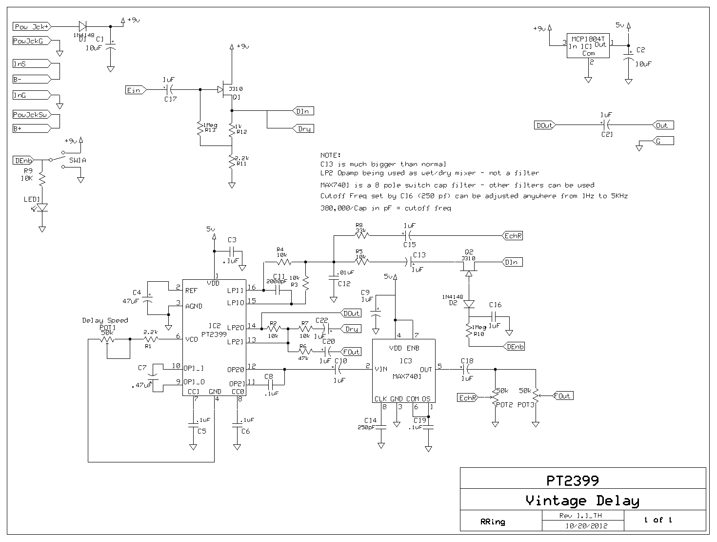
Lots of great PT2399 designs out there….. I have tried a number different variations and have built what I consider a best performance design, using a compander, elaborate filters, etc. I have been frustrated as many builders out there are – that the PT2399 is so easy to use but that it just goes to crap with longer delay times! So I decided to work and experiment with different approaches to converge on a simple, yet well performing design. I am really happy with what I have come up with.
The design uses a discrete FET input buffer and uses one of the on board op amps as the wet/dry mixer. The dry signal always passes through and the effect is defeated by just opening the connection of the signal input to the delay chip. This allows “tails” or the echos to naturally decay even when the delay is bypassed. There are two features that make this circuit perform really well. One, the cap between pins 9,10 is made much larger than typical in other designs and the data sheet reference design and two, I use a 8 pole switch cap filter IC for the post delay aliasing filter. The larger cap provide significant increase in the delay output but the noise remains at the same level. I then attenuate the output in the wet dry mixer to the normal level this also downward expands the noise. The switch cap filter is really simple, requiring only one capacitor to set the corner freq from 1Hz to 5KHz. It is very easy to implement and has excellent performance. The total circuit rivals the simplest bare bones designs but approaches the performance of the more advanced circuits such as the PT80 delay.
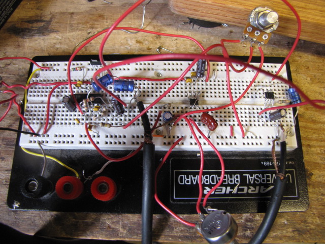
Below are the schematic, a picture of a breadboarded prototype and some example audio of the prototype below, in use.
Updated Version in pedal form
Schematic: https://circuitsalad.com/wp-content/uploads/2012/12/analog-delayschematic1.gif
Picture of Prototype: https://circuitsalad.com/wp-content/uploads/2012/09/delay_proto.jpg
Sound Sample: https://circuitsalad.com/wp-content/uploads/2012/09/delay-demo.mp3

Hey! I really like idea of re-purposing the amps. I want to build a v.simple delay and resonant filter module for a modified keyboard. My plan was to use one of the amps in the pt2399 to do the job of the amp in this super simple VCF by Tim Escobedo: http://folkurban.com/Site/QDVCF-714.html
Do you think it will work? Cheers!
Yes it will work fine but do keep in mind the headroom is low because they work off of 5 volts and you only have access to the neg input and output.
Good Luck!
great, i’ll breadboard it up. i was thinking of having a switch to toggle between the first amp being a nice sounding filter (as you have) to the vcf for squarking and parping. so i can still use the second for mixing. BTW i am a bit daft, what do you mean specifically by ‘keep in mind low headroom they work off of 5 volts and you only have access to the neg input and output’ ?
Thanks again!!
since the supply is only five volts – you can only swing +- 2 volts or so(on the output). If you have any significant gain – it could clip. The internal op amps have hard wire the + inputs to a mid supply bias and ac ground so you only can use the an inverting op amp topology.
On Mon, May 20, 2013 at 5:18 PM, Circuit Salad
Fantastic well improved that’s how a pt2399 should sound like not muffled like some designs and sounds.
Well done.
Oh by the way I have a design would it be possible fir you to get in touch with so I can show you and from there we can make improvements.
Cheers
vim
Yes I am really pleased with the result. I need to do another layout better suited for home brew PCB’s and post. Currently I have a link for the current PCB layout in ExpressPCB – https://circuitsalad.com/category/audio-electronics/pt2399/. This layout is fine it just would be more tricky than it needs to be for home brew. To view you will need to download expresspcb’s free layout tool
Hi Ray, here Mark from France. I just built the improved version to put with a home assembled theremin (Theremax from Paia). I made a PCB myself, using Altium, with all resistors vertically to have a smaller PCB. Works very well indeed. I love the feature that the contents of the delays goes on when you turn the delay off. Just a message to let you know that also from this side of the ocean you have admirers. Great job you do, while sharing the information!! I built a couple of them, in order to give them to musical friend….Greetings, Mark
I am so glad it works for you! There are a number of simple PT2399 delay designs out there but they just don’t work that well. Yes I have started doing the resistors vertical also and it definitely helps with the layout. I have more stuff in the works so hopefully some of it will be of use to you in the future.
This sounds great on your mp3 samples. I need some ambience for flamenco with my super lightweight DIY buskers boombox, which uses one of those small rucksacks with a folding stool attached meant for artists or fishing kit. Keeps the amplification discreet. Your design should work very well for this. I’m unclear about what exactly the second FET does and don’t have any in the scrapbox at the moment.
Can I leave out the FET buffer since I already have a pre-amp output from the ceramic bridge pickup?
How are you switching the loop effect in your video?
In this circuit, the output is always connected to the delay effect. The input is connected/disconnected via Q2 to the input of the delay circuit. This way a tails feature is provided. You only need Q1 to provide low Z drive buffering the the delay chip. If your input is already buffered you don’t need Q1..except to bias Q2 to half supply. so you will need to replace Q2 with a bypass switch or bias it with a couple resistors.
The relatively expensive rail to rail opamp could be replaced with a single supply LM324, if a simple zener regulated 7.5 volt supply was provided for it? I have dozens of LM324s and they swing to 0v. The 2399 bias ends up on the non-inverting input, therefore it will still keep the signal in the right place to get sufficient output +v swing, but still without using an input decoupling cap?
I don’t understand your questions exactly because there are no op amps in my circuit, nor do I understand the 7.5v zener and why it would be used. In general, yes you can use the existing bias of previous stages and direct couple.. I do it all the time.
Thank you for the clarification on Q1 and Q2 roles. My question about the opamp should have been made clear that it was the ‘alternate analog filter circuit’ I was referring to. Sorry about that. The zener diode is just a way to provide a supply rail which gives the same output voltage swing as your original choice of opamp. I am powering the main amp and delay from a 20v NiMH battery pack.
Got it – sure you can use any beef stew op amp and eliminate the buffers
I built your circuit on pad board and it works great using the alternate analog filter with an LM324 and seperate regulated 12v supply. Thanks so much.
It works so well, that I couldn’t help spicing it up. With a 555 timer in the scrap box already on a tiny PCB from a broken alarm flasher – output to an LED in a black tube glued to an LDR wired across the time pot. So the delay time and modulation depth can be varied with two more pots.
The only issue i want to ask you about is what might be wrong with the Q2 section – if I flip the switch the delay repeats fine, but when I go back or often when I connect power, it takes ages for the delay signal to start coming through the mix. If I turn the repeats pot right up, everything is definitely running on the PT2399 which starts to build up in feedback. Double-checked FET, diode, resistor, dry joints etc. With cap and resistor values you give, the time-constant should be around 0.1 second?
Let me check the schematic again. Using a jfet as a analog switch is pretty straightforward so – it will work reliably. The RC time constant is just to eliminate clicks – it not critical to the switch behavior itself. It is important that the jfet sees a DC bias – which sets the signal swing range across it. I will look it over again and make sure I don’t have any errors and will get back to you.
Just a clarification. RC time constant is .000001*1000000 = 1 sec not .1sec. I would check the input to the FET from Din(from the other input FET’s source …make sure is near 1/2 supply and not capacitively coupled).
Also make sure diode D2 is in the correct orientation.
Ofcourse if you have a a 10meg resistor by mistake or a 10uf cap that would do it also.
Understand – I realize you are not stupid but I don’t know what else to do but just throw out ideas to sanity check
Hi! I’m very interested to try your circuit, but I’m slightly confused with the labelling on the schematic… Is ‘pot2′ the number of repeats?, and the input is ‘DIn’ on the right? Or does ‘DIn’ connect with ‘DIn’ What’s ‘Ein’? And ‘Dry’ connects with ‘Dry’, ‘Denb’ with ‘Denb’, and ‘FOut’ with ‘FOut’? What does the ‘FOut’ pot (pot 3) do? Is ‘DOut’ the main output?
Thanks for your patience!
So no problem with the questions..Some others have told me my schematics can be confusing…sorry about that. My schematics relate to my layouts and with pedal assembly in mind. Let me clarify for you.
first off here is a simplified schematic link: https://circuitsaladdotcom.files.wordpress.com/2015/02/analog-delay_simple.jpg
So the dry signal is a buffered input signal and is always connected to the output(by means of an internal op amp within the PT2399). Denb, when grounded passes the input through the delay circuitry. So Denb goes to your stomp switch. This way of doing it is to support the Tails feature. You could eliminate this and do a standard bypass circuit. If it would help I can provide this alternate approach schematic.
Ein is the actual input connected to the jack, Fout controls the level of delay effect in the mix and is connected to an op amp within the PT2399(using it as a mixer) Dout(delay out) is the mixed dry and delay signals and is the final output(goes through cap and is named Eout (effect out). Pot 2 is the repeat level as you concluded.
Look at the simplified schematic link …that will also help.
Just finished the circuit! Works great! Only one question.. Which type of pots are you using? Log or linear?
I’m using linear pots. The delay time definitely should be linear. The others may not matter much but I like just using linear
Thanks!
I have to say it again,but this echo unit sounds great! Thanks for the schematic! Although while playing with this echo unit, I came across with two issues, I had to improve to fit perfectly to my personal taste.. 1st How can I get even slower repeats/time? And 2nd How can i get a wet/dry feature in this circuit? Do you have something tested in mind?
wet/dry?split dual output..is that what you trying to do? Slower repeat time …change the 50k delay time pot to 100k but you will get grainery repeats at the slow times
So if I cut the dry signal from pin14 & pin13 will I get only the wet signal from the output?
yes you can do that. pins 13 and 14 are a utility op amp available on the pt2399 – I am just using as a mixer to combine the dry and wet
Ok, If I try this I’ll let you know the results! And one last thing, have you measure the in/out impedance? Again, thanks for everything!
1 meg in….probably 200 ohm or so on output
Hi there, still working on your design, the only problem is that I can’t achieve slower repeat time: any bigger tpot except the 50k you originally suggested produces a huge continuous noise.. Any suggestions?
yes that is the problem with this chip. In fact typically getting more than 300 mSec is not achievable. My design is intended to improve this significantly but there is still a limit. The problem is that to get longer delays you slow down the clock which greatly reduces frequency response because of sampling error. You only solution is to cascade the chips effectively doubling your memory for a given clk speed
Hi! Nice work!
I’m new to building circuits, but if I would like to add a feedback loop, should I add something in between, or should I just feed it back into the circuit “as is” ? I would like to make infinite “loops” with it.
It does infinite loops as designed just turn up the repeat knob. Keep in mind…it sonically deteriorates as the repeats continue because the output is looped back into the input as analog and does not stay in the digital domain such that it can be repeated forever with no degeneration.
Hi there! One more question.. Which is the correct polarity for cap13?
positive is on pin 10 negative on pin 9
thanks for the answer! The second unit i built, the feedback wan not infinite, although it was the exact same design as the first one. I noticed by accident that when i try to desolder the 100n capacitor between pins 12 & 11, infinite feedback came on again. Every single time i warm up the capacitor feedback was infinite, when it cooled down feedback fade out again.. My thought is that heat changes it capacitance, so that happens. except the cap between pins 9&10 what else are the parameters that affects infinite feedback?
Nice project, thanks! 🙂 How the larger cap (pin9,10) increase the out level? It seems It’s bypassing the inner 4k7 resistor of OP1 (It works as integrator maybe. The datasheet doesn’t specifies it)
Hello Ray, here Francisco from Argentina, thank you very much for your ideas and projects.
I built the alternative version, same topology, 8th poles, LM324, 2.3 Khz and it works perfectly. But I’m going to try MAX292 and MAX296, here I can not get 7401 or 7405. I saw you added SA571 in Hell Dice delay, I wanted to ask you if it’s really worth it, with NE571 I could not get a big difference in total performance.
And a final question, what do you think about cascading the TPA5050-5052, with almost 200 ms (digital stereo audio input) for this type of delay projects?
Regards!
hey there yeah the 571 helps a little for the first few repeats…not sure it worth it but …gave it a try. Those parts are cool! you have an extra op amp available which is nice. TI part is interesting…I never played with it …will have to look into it
Just found this great circuit today. I have a question: in the first circuit I downloaded, C13 was labelled as C7, and the positive was on pin 9.
The simplified circuit shows C7 as C13 now and the polarity reversed so the positive was on pin 10.
Which one is correct? is pin 9 positive as on cct 1 or is pin 10 positive as on the simplified cct?
Im a little confused.
I don’t think it matters to much but you can use a non polarized cap or …I think it is best to have the positive side of an electrolytic going to pin 9
Ok thank you
hi, me again. i am a little bit confused about the bypassing/dry-wet mixing.
we have a mix pot, ok, but i can not understand how to wire the bypass with the footswitch.
ty
C19 is a 2000pf non polarised capacitor. Would it be ok to use a 2uF electrolitic, its all I have?
Hi, I built the circuit from your simplified diagram. I made the circuit board using EastEDA, but I couldnt get it to work. The switch doesnt do anything, and all I get is the guitar playing straight through.
So I rebuilt the circuit using strip board and I get exactly the same results. Is your drawing of the circuit board accurate and has anyone got it working from this schematic?
I dont know what to try now if your circuit diagram is accurate, get you give me any pointers?
Thanks
Chris
Hm same here, but i do get a very quiet output signal from the 2399, only the dry signal is way louder.
Dont know
Let me look at this, others have built this successfully
Can you explain the function of D2? It looks to me like it would block the current needed to turn on Q2, but I’m self-taught and still learning, so probably just missing something.
So this is a field effect N channel JFET used as an analog switch. This device functions based of fields not current flow like a bipolar transistor. We define the input side as the source connection and the output side is the drain. When the gate is negative with regard to the source, the FET is open and no signal flows. The source is biased to approximately 1/2 supply by means of the direct connection to the input buffer, so when we ground the gate, it becomes 4.5 volts negative with respect to the source and shuts off the FET . If we connected the gate directly to 9 volts without the diode….the FET would turn on but the inherent diode of the junction FET would conduct as the PN junction from gate to source would have 9-4.5v across it. This would interfere with circuit operation. By adding the reversed diode the junction is brought up from the negative state(when connected to the 9v) by means of diode leakage current only until both the gate and the source are at 4.5 volts. With zero potential between the gate and source the JFET is fully on. It does not have to be forward biased only made non negative.